
Executing the Operation
Initialization
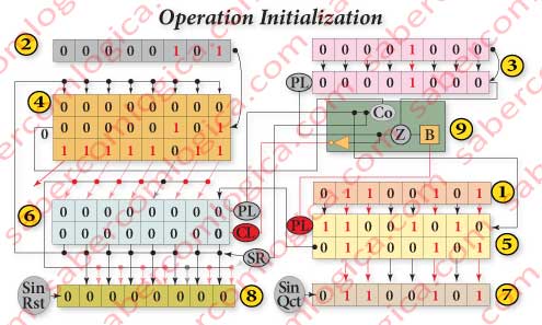
In this first figure we’ll identify the symbols and components used and assign them their initial values. For the symbols we have:
- Sin Qct – Quotient sign
- Sin Rst – Remainder sign.
- B – Circuit for analysis of Zero Detection.
- CL – Register Clear Signal (active at 0)
- Co – Adder circuit Carry out.
- Z – Signal indicating the Zero Detection (active at 1).
- PL – Signal indicating the selection of Parallel Load (active at 1). We’ll call PL3 to the one of Counter 3, PL5 to the one of Register 5 and PL6 to the one of Register 6.
And for the components:
- 1 – Represents the Circuit 1 and contains the dividend value converted to an unsigned integer 01100101(101) for our operation. It’s connected to the MUX load input of Register 5.
- 2 – Represents Circuit 2 and contains the divisor value converted to an unsigned integer 00000101(5) for our operation. It’s connected to the 2nd operand of Adder 4.
- 3 – Represents Counter 3.The upper row contains the iterations to load when a zero detection happens, 00001000(8) the dividend bits.
The lower row contains the memorized value. It has just loaded the iterations’s number 00001000(8). - 4 – Represents the Adder 4.
The upper row contains the 1st operand always coming from Register 6. It’s initialized with 00000000(0).
The middle row contains the divisor here remaining unchanged until the end of the operation with the value of 00000101(5).
The lower row contains the operation result which is connected to the MUX’s load input of Register 6 as described in its implementation. Now it’s 11111011(-5) and irrelevant.
From the circuit left side comes the operation Co, connecting to Frame 9. At this step is 0 (it doesn’t fit). - 5 – Represents Register 5.
The upper row contains PL value selecting the MUX input for the next clock (shift or load). In this step it’s the left shift 11001010 of the memorized value. The lower order bit value isn’t the one to be admitted, as only after our last relay racer arrives and the clock falls it’s value will be known.
The lower row contains the memorized value. It’s initialized with the dividend value, thus loading 01100101(101). The bits being admitted to the quotient during the operation are highlighted in bold. - 6 – Represents Register 6.
The upper row contains PL6 value selecting the MUX input for the next clock (shift or load). In this step it’s chosen the left shift 00000000 of the memorized value, as the bit being admitted is 0.
The lower row contains the memorized value. It’s initialized through a Clear (CL) to the Register, reason why in this step it’s value is 00000000(0). The bits being during the operation are highlighted in bold. - 7 – Represents Circuit 7. During the operation it will show the values resulting from its connections, but only at the end of the operation it will show the operation Result. The intermediate readings are meaningless.
- 8 – Represents Circuit 8. During the operation it will show the values resulting from its connections, but only at the end of the operation it will show the operation Remainder. The intermediate readings are meaningless.
- 9 – Represents the Control Unit 9, which doesn’t show any values. They are evinced by the color of the lines.
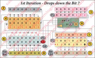 First Iteration
At the Clock’s rise:
The Register 6 left shifts, admitting the order 7 bit of Register 5, which was set in its input during the previous step. It’s now that the dividend’s 1st digit (0) drops down.
The Counter 3 decrements one unit and shows 00000111(7).
When the Clock is high:
The Adder 4 1st operand assumes the value of Register 6 outputs, showing the algorithm Frame 7 result, 0 11111011 . This result is irrelevant as the divisor doesn’t fit. Co is 0, it’s value being prepared to be admitted by Register 5.
At the Clock fall:
When Register 5 left shifts, it admits the newcomer bit with Adder 4 Co value, as the quotient 1st digit (0).
When the Clock is low:
When Register 5 left shifts, it’s highest order bit now being the dividend order 6 bit, propagates to the lowest order bit of Register 6 inputs, where it waits for the next clock rise to be memorized, i.e. for a new iteration to be dropped down.
We can see in Figure 1 the evolution with the Clock the values of Register 5 and Register 6.
 Second Iteration
The Counter 3 decrements and shows 00000110(6).
The Register 6 left shifts and receives the dividend order 6 bit, i.e. it’s 2nd digit (1) is dropped down. The result is sent to the Adder 4 1st operand, where the algorithm Frame 6 operation is executed.
The divisor doesn’t fit.
The result is irrelevant, Co is 0 and its value it’s going to be received by Register 5 as the quotient 2nd digit (0) when it left shifts and sets the dividend order 5 bit in Register 6 input.
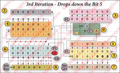 Third Iteration
The Counter 3 decrements and shows 00000101(5).
The Register 6 left shifts and receives the dividend order 5 bit, i.e. it’s 3rd digit (1) is dropped down.
The result is sent to the Adder 4 1st operand, where the algorithm Frame 5 operation is executed.
The divisor doesn’t fit.
The result is irrelevant, Co is 0 and its value it’s going to be received by Register 5 as the quotient 3rd digit (0) when it left shifts and sets the dividend order 4 bit in Register 6 input.
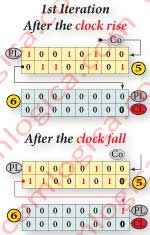
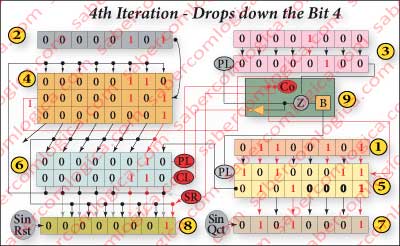 Fourth Iteration
Counter 3 decrements and shows 00000100(4) iterations to go. Register 6 admits the dividend order 4 bit do, i.e. its 4th digit (0) is dropped down and the result is sent to Adder 4 1st operand, where the algorithm Frame 4 operation is executed with 1 00000001 as Result. Now the divisor fits. Co is 1 and PL6 becomes 1, selecting the left shifted Result value into Register 6 inputs. When Register 5 left shifts it admits the newcomer bit with Co value as the quotient 4th digit (1) and sets the dividend order 5 bit at Register 6 input 0.
In Figure 2 we illustrate how the changes in Register 5 and Register 6 evolve with the clock in this 4th iteration, as they are not visible in the frames representing each iteration final situation. Let highlight the most significant of them:
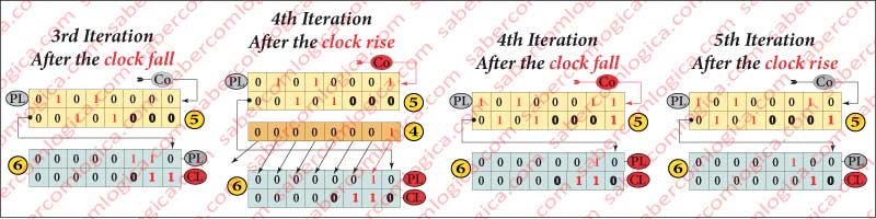
After the clock rise and the resulting changes propagation, the bit in Register 5 changes its value. Actually, when the clock rises the Register 6 left shifts, propagating the new memorized values. In consequence the Adder 4 1st operand’s value changes and so does the operation Co, which in turn propagates itself to the Register 5 order 0 input, where it keeps waiting for the clock fall to be memorized in it.
The value shown to PL6 in the final situations frames doesn’t refer to what it did in that cycle but to what it’s going to do in the next cycle. Notice that only after the propagation of Co new value PL6 will change it’s value forcing the Load of the operation’s Result into Register 6 when the clock falls.
After the clock fall and the resulting changes propagation the Register 6 order 0 bit changes, in our case from 0 to 0, keeping its value only by chance.
Actually, when the clock falls the Register 5 left shifts and sets a new value at its order 7 bit ,which in turn propagated its value to the Register 6 order 0 bit, where it stays waiting for a new clock rise.
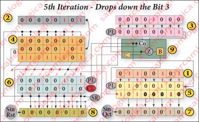 Fifth Iteration
The Counter 3 decrements and shows 00000011(3) iterations to go.
The Register 6 left shifts and receives the dividend order 3 bit, i.e. it’s 5th digit (0) is dropped down.
The result is sent to the Adder 4 1st operand, where the algorithm Frame 3 operation is executed.
The divisor doesn’t fit.
The result is irrelevant, Co is 0 and its value it’s going to be received by Register 5 as the quotient 5th digit (0) when it left shifts and sets the dividendorder 2 bit in Register 6 input 0.
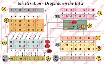 Sixth Iteration
Counter 3 decrements and shows 00000010(2) iterations to go.
Register 6 left shifts and admits the dividend order 2 bit, i.e. its 6th digit (1) is dropped down and the result is sent to Adder 4 1st operand, where the algorithm Frame 4 operation is executed with 1 00000001 as Result.
Now the divisor fits.
Co is 1 and PL6 becomes 1, selecting the left shifted Result value into Register 6 inputs. When Register 5 left shifts it admits the newcomer bit with Co’s value as the quotient’s 6th digit (1) and sets the dividend’s order 1 bit at Register 6 input 0.
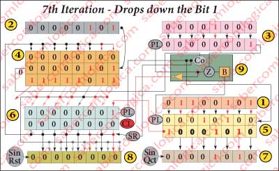 Seventh Iteration
The Counter 3 decrements and shows 00000001(1) iterations to go.
The Register 6 left shifts and receives the dividend’s order 1 bit, i.e. it’s 7th digit (0) is dropped down.
The result is sent to the Adder 4‘s 1st operand, where the algorithm’s Frame 1 operation is executed.
The divisor doesn’t fit.
The result is irrelevant, Co is 0 and its value it’s going to be received by Register 5 as the quotient’s 7th digit (0) when it left shifts and sets the dividend’s order 0 bit in Register 6 input 0.
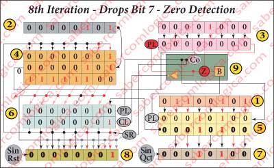 Eight Iteration
The Counter 3 reaches Zero.
Figure 3 , illustrating the evolution of the variables values and of the circuit states from the clock rising edge of the Zero detection cycle until the clock falling edge of the 1st iteration cycle, will help us following this description.
When the Clock rises:
The Counter 3 decrements and shows 00000000(0) iterations to go. The Register 6 left shifts and admits the dividend’s order 0 bit, i.e. its 8th digit (1) is dropped down.
While the Clock is high:
The value in Counter 3 outputs propagates to its NOR gate and Zero Detection happens. Z becomes 1, propagates to Circuit 9b where it will stay at the delay ETL input, sets PL3 to 1 and CL to 0 (CL=¬Z).
The value in Register 6 outputs propagates to Circuit 8 MUX input 0 as the Remainder 1st possible value 00000001 and to the Adder 4 1st operand, where the algorithm Frame 0 operation is executed. The divisor doesn’t fit.
The Result propagates to Circuit 8 MUX input 1 as the Remainder 2nd possible value 11111100.
Co is 0, propagates to Register 5 input 0 and sets SR to 0, thus selecting Circuit 8 MUX input 0 (the values memorized in Register 6) where the Remainder final value stays.
When the Clock falls:
When Register 5 left shifts it admits the Adder 4 Co newcomer bit as the quotient 8th digit (0). The quotient final value is now memorized in this Register.
While the Clock is low:
The value memorized in Register 5 propagates to Circuit 7 where it will be the Quotient final value.
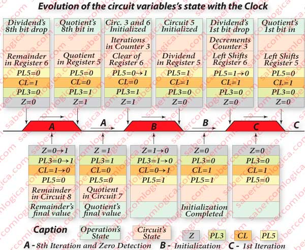
When this 8th iteration cycle is finished, the circuit variables with the values
Z=1, PL3=1, PL5=0 e CL=0
are ready for the initialization cycle which is coming.
We are going to repeat its description emphasizing the variables values evolution and its influence in the circuit states.
Initialization after Zero detection
When the Clock rises:
As CL is 0, a Clear is made to Register 6. As PL3 is 1, the new iterations number is loaded in Counter 3.
While the Clock is high:
The value of Counter 3 outputs propagates to its NOR gate, where Z becomes 0 and propagates to Circuit 9b. There it stays at the delaying ETL input and sets PL3 to 0 and CL to 1. The delaying ETL output becomes 1 and propagates to PL5 which becomes 1.
When the Clock falls:
PL5 being 1 forces Register 5 to load the dividend new value.
While the Clock is low:
Register 5 highest order bit propagates to Register 6 lowest order bit, where it waits as the 1st dividend digit to be dropped down. The circuit is now fully initialized. The variables values are:
Z=0, PL3=0, PL5=1 e CL=1
First Iteration (New Operation)
When the Clock rises the Circuit 9b delaying ETL output becomes 0 and propagates to PL5, so becoming 0. The variables values are now
Z=0, PL3=0, PL5=0 e CL=1
remaining like this until the next Zero Detection.