How the CPU Works
As a support to our work we are going to develop a very basic CPU with a word size of 8 bits and with a very limited instruction set, namely 16. With 8 bit, 256 memory locations or bytes can be addressed. Thus, the memory can have a maximum size of 256 Bytes.
We tried to show how with actually only one memory, through the L1 cache, the CPU can address two separate memories, data and instructions. Of course, if memory has 8 bits per position both L1 caches must have 8 bits each. But this is the reality. Our CPU will have two distinct memories with 256 possible positions each.
The Data Memory (DM) will have 8 bits per position and the Instructions Memory (IM) will have 12 bits per position. We will understand further on why this difference an why the CPU Registers (the word)will keep the same 8 bits width.
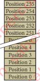
In our imaginary the Memories will have their positions arranged in stack, as shown in Figure 2, where each position is defined by a sequence number starting at 0.
The Data
The ALU is able to execute logical and arithmetical operations according to the circuits it incorporates like counter circuits, bit shifting circuits, arithmetical circuits, logical circuits, and so on, some of whom we’ve already analyze.
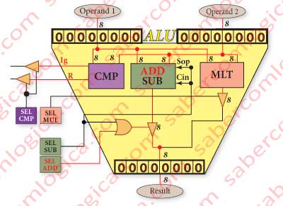
For our CPU we are going to admit that the ALU as the ability to execute 4 operations: addition, subtraction, multiplication and comparison, for what it will include the Adder/Subtractor, the Multiplier and the Comparator circuits.
We can see this description into Figure 4. The number 8 near one line means that it represents 8 bit lines. The number 1 means that it represents 1 bit line.
But how are we going to tell the ALU what operation to choose in each situation?
Selecting an Operation
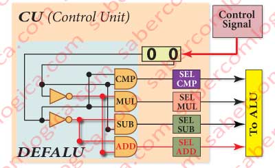
All the operations circuits have their outputs simultaneously converging to the ALU outputs, but only one of them can be there at each moment. In order to get this we must interpose Tristate gates active to 1 in each one of the bit lines coming from each of the operations circuits. It’s through the activation of these Tristate gates that we’ll tell the ALU what operation to choose. In order to select them separately by circuits we’ll use a DEMUX with 4 outputs, one for each of the adding, subtracting, multiplying or comparing operations.
It will be a 1 to 4 DEMUX having each one of its outputs connected to each circuit set of 8 Tristate gates, thus activating each set through the activation of its output connected to it. For such a DEMUX we’ll need a 2 bits selection control. We’ll call it DEFALU (DEFine ALU‘s Operation) which will select the addition (00), the subtraction (01), the multiplication (10) or the comparison (11). We can see in Figura 5 the graphic representing the composition of this DEFULA.
This is the first step to build the Control Unit for our CPU. It’s in this unit that the signals which will control the CPU operation will be defined and issued. Now we have the solution to tell the ALU the operation it has to run. But it needs operands to do an operation.
How can we get the operands for the operation?
Getting the Operands
The strong connection between the CPU and the Memory will be noticeable from now on.
For our CPU, as a way to turn easier the intended, to understand the CPU, we will consider the Memories as being circuits integrated in the CPU, thus existing a direct and immediate communication between CPU and Memory. The real way how the communication between the CPU and the Memory is done doesn’t matter at this point of our work, but it will be profusely treated in future Chapters, due to its complexity and importance.
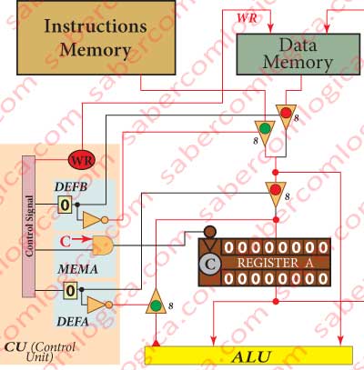
The CPU is in permanent communication with the Data Memory (DM) and works only with data registered there. So, the operands are obtained from the DM. To control the operating mode executed over the DM we’ll have the WR (WRite) signal, active to 0. This will be the only signal used to control the accesses to the DM.
- When active (WR=0), it’s written in the DM, at the designated address, the value at its input.
- When inactive (WR=1), the value registered at the position designated by the address will be available at the DM‘s output.
The referred address will be obtained from the content of instructions commanding accesses to the DM, as we’ll see further on. For now it’s enough to know it.
We start by reading the 1st operand from the DM. But the ALU needs two operands in order to do an operation, and we can only access one for each DM reading. So, the 1st operand must be kept somewhere inside the CPU core while we read the 2nd operand.
It’s now time for the Computer Registers to come into play in our history.
In order to temporarily keep the data needed for our CPU’s operations we will introduce a Register into it, the Register A which we will call by RegA from now on. The 1st operand will be kept into RegA after it is read from the DM.
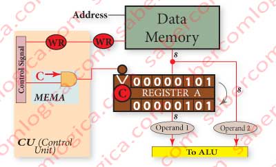
For data to be memorized into RegA, it has to be connected to the DM‘s output and receive a controlled Clock signal active when that must happen. That controlled Clock will be achieved by MEMA (MEMorize in A).
MEMA is active to 1, as it will be the clock for RegA. Connecting it together with the Clock signal to an AND gate, we can ensure that only when MEMA is high (1) the Clock acts on RegA, memorizing and propagating its input to the ALU 1st operand, as exemplified in Figure 1-6.
Once saved the 1st operand, we can now read the 2nd operand value from the DM, by connecting the DM output to the ALU 2nd operand . Thus, when addressed the DM position where it lies, its value will be available at the DM output, propagating to the ALU as the operation 2nd operand.
Figure 6 describes graphically the introduction of Register A and two more control signals to be defined and issued in the Control Unit.
Executing the Operation
The 1st and 2nd operands operating in the respective inputs of the ALU, by propagation of their signals. This same propagation sets the result of any of the ALU circuits operations in their respective output, and the selected one at the ALU‘s output. Let’s follow this description with Figure 7. As during this cycle the 2nd operand is being read from the DM, the WR signal is inactive for writing. Thus, the operation’s result can’t be written in the DM and we’ll have to write it temporarily in RegA, overriding the 1st operand’s value.
In order to do it, the ALU’s output will be connected to RegA, further propagating the operation’s result to its input. And there its propagation stops. It arrived to a Register and the door is closed.
Besides this result, the ALU circuits provide us with some other kind of information which is essential to the interpretation of the result itself.
This information provided in parallel by the ALU are for instance the bits informing about the existence of Cout (Carry Out) and Exs (Excess) or the bits Ig and R telling about the state of the compare circuit, among others.
Any of this signals tells about the state of the ALU circuits besides the result they can provide. And they will tell about their value to a Register, the RegALU (ALU Register), which we can see in Figure 8. We included in the information provided by the ALU to the CPU only the bits Ig and R resulting from the comparison, because they are the only ones we are interested in, for now.
The Register A and MEMA
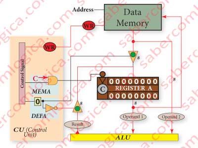
So, the RegA will be connected to the DM output and to the ALU output, i.e. two sets of 8 bit lines are converging to its input. Since only one of the two sets can be present there at a time, we’ll intercept these lines with Tristate gates.
How to tell RegA, when MEMA becomes active, whose of the sets it must memorize?
We are facing a conditional decision, to be solved with the DEMUX A. With its 1 bit control signal it will activate one of the sets of Tristate gates. We will call DEFA (DEFine A input) to this control signal.
When the value memorized in RegA is not useful for the coming operation, it’s time to save its value into DM. Connecting its output to the DM, its value will be saved at the designated address when WR is active (WR=0),as we can follow with Figure 7.
Responsive to What Clock Edge
The question to be analyzed is how to ensure that when MEMA acts as Clock on RegA, the value that will be memorized in it will be the one we want.
Every signal has a propagation time within the circuit, as bigger as the distance they must run and the number of transistors gone through.
The rising clock in RegA only happens when the value 1 of MEMA gets to the AND gate and lets the real Clock, when it is high , propagate. And that’s when the Clock will rise in RegA and the value in its input is memorized.
Notice what we have said: the rising clock in RegA doesn’t happen when the real Clock rises, but when it is high.
What value will be at its inputs when it happens? Is it possible that, for instance, when we want to memorize the operation result it isn’t yet arrived at its input? Who knows?
Well, but the action of MEMA as clock over the RegA will be repeated when the real clock rises for the next cycle, as at that precise moment the value of MEMA will still be 1. And then the intended value will already be there.
Who can assure us that in the meanwhile, before the 1st action of MEMA as clock on RegA, the value present at its input isn’t changed?
Yeah! And if that happens the ALU 1st operand changes and in consequence the result present at the input of RegA to be memorized at the next Clock.
Everything would be mixed. Thus, we remain in doubt.
The solution resides in synchronizing the real Clock event with the MEMA induced clock event. For this to be possible, MEMA has to be already active (1) when the real Clock event happens. And it will actually happen when the Clock falls.
Therefore, the RegA will be a Register sensitive to the Clock’s falling edge.
The Instructions
Now we know how the ALU operates, how it gets its operands, what we do with its result and how we operate with the DM. We defined some command signals
DEFALU, MEMA, WR and DEFA.
The question now is how we do we designate their value.
That’s the role of the instructions we’ll provide to the CPU, which will arise the CPU ability to turn a computer other than a washing machine. Each instruction must specify the necessary values to execute each operation and is be the content of the IM position where it lies.
Each instruction by itself doesn’t produce much, reason why they are used in groups and ordered according to a certain sequence: the Program. A program runs according to the natural sequence of its instructions, kept in the IM with that same sequence.
The same way it happens with the DM, the IM needs to be told the address where lies the instruction to be executed. For that purpose the CPU has a pointer.
The Program Counter
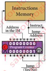
The PC (Program Counter) is the instruction’s pointer, always containing the address of (it points to) the instruction being executed in the IM. The PC is a CPU Register and in our CPU it will be represented by the PC.
The instructions are read from the IM according to their natural sequence. The PC is incremented for each executed instruction and will then point to the next instruction to be executed. So being, it will be an ascending binary counter.
In any program there’s conditional or unconditional jumps. Jump is a deviation from the program normal execution sequence.
- An unconditional jump happens when it’s executed an instruction whose function is to divert the program’s normal execution sequence to another location designated in the instruction itself.
- A conditional jump happens when it’s executed an instruction whose function is, through the analysis of a specific condition, to divert or not to divert the program’s normal sequence to another location designated in the instruction itself.
Therefore, when a jump happens according to an instruction content, the program natural execution sequence must be changed to an address which is part of the instruction itself. Thus, the PC must be loaded with that address where the new program execution sequence starts. For this reason the PC will be an ascending binary counter with parallel load.
In Figure 9 we show the set PC and IM to be included in our CPU. And its precisely from the analysis of this figure that comes the next question:
How is the PC told that there’s a jump and that it must execute a parallel load?
Jumps or Increments
Jumps if zero, jumps if less than zero, jumps if less then…, jumps if greater then …, jumps if equal to …, jumps if different from…, etc., are some possible instructions of conditional jump. They are the analysis of expressions (the predicate) comparing two variables and/or constants returning a true/false result, i.e. jumps or doesn’t jump.
This is why we added a comparing circuit to our ALU. We recall that it returned two 1 bit signals as the result:
- Ig being 1 when A and B are equal.
- R being 1 when A greater than or equal to B or 0 when A is less than B.
In our case study A represents the 1st operand and B represents the 2nd operand. So, with the Ig and R values returned by the ALU we are now able to take decisions.
In our CPU we want to introduce 3 jump conditions:
- If A is equal to zero, where A is compared with B, assuming B the value 0. If Ig is 1 then A=0 and so being jumps.
- If A is less than B, where A is compared with B. If R is 0 then A
- If A is negative, where A is compared with B, assuming B the value 0. If R is 0 then A
In the PC we will make PL active to 1.
- When PL is 1 the address of the instruction to execute, the one where to jump, is loaded.
- When PL is 0 the address of the instruction to execute, increments.
For our CPU we will admit 4 different possibilities for the addresses evolution: Jumps if less then, Jumps if equal to, Jumps unconditionally or Increments. From these 4 possibilities a value must result to PL. A MUX with the 4 possibilities in its inputs solves this.
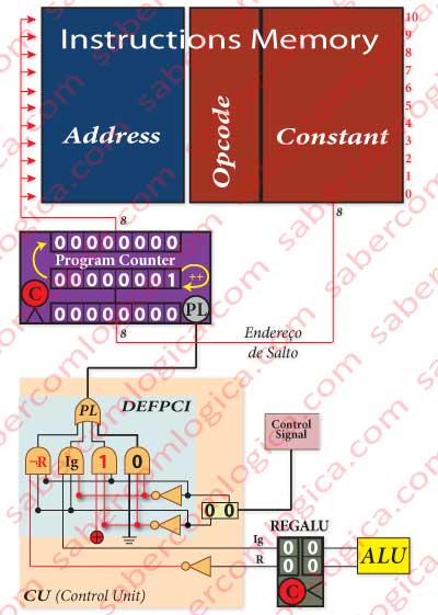
We will call it MUX PC and to its 2 bits selection signal DEFPCI (DEFines PC Input). We can see it represented in Figure 8.
In the MUX PC inputs (X0,X1,X2,X3) we’ll have:
- In X0, the value 0, selectable with DEFPCI(00) resulting in PL=0 and in the PC increment.
- Em X1, the value 1, selectable with DEFPCI (01) resulting in PL=1 in a PC jump.
- Em X2, the value Ig returned by the ALU, selectable with DEFPCI (10). Se A=B then Ig=1 thus PL=1 resulting in a PC jump. Se A≠B then Ig=0 e thus PL=0 resulting in the PC increment..
- Em X3, the value ¬R returned by the ALU, selectable with DEFPCI (11). Se A
When it jumps how do we tell it about the address where to jump?
How the Instruction is Composed
The instruction read from the IM is composed by
- a 4 bits space for the code representing the 16 instructions set and
- an 8 bits space for the adress or any other value, as this is the CPU Registers width
thus having the IM 12 bits for each position.
Always an instruction orders a jump the MUX PC must be told about the address of the position where to jump, reason why that value will be included in the 8 bits space of the instruction. Thus, the IM lowest order 8 bits must be connected to the PC parallel load input, where to it will propagate to be read when necessary, as in Figure 8.
If the instruction doesn’t order a jump its 8 bits space will be empty, as there nothing to tell to the PC. It will increment thus operating like an ascending binary counter.
But that space will not be empty as there are other uses for it. When writing a program is sometimes necessary to designate in the instruction itself, a value for the operation to be executed in the ALU or the DM address where to read or write.
As an instruction ordering an operation in the ALU or ordering to read or write in the DM doesn’t surely order a jump, the 8 bits space will be vacated and we can fill it with those new values.
The Constant
From now on we’ll call constant to the value contained in the lowest order 8 bits of each IM position .
From what we have seen so far, this constant can have several meanings and will have to be linked to several places. For now it can be an IM address, an operand for the ALU or a DM address. Thus, the constant will be connected to:
- The DM address input.
- The PC parallel load input.
- The ALU if it’s its 2nd operand.
- The RegA if it’s the ALU 1st operand.
As in these two last inputs there’s already a connection to the DM where we will interpose the MUX B, whose task is alternatively activate the tristate inserted in the bit lines coming from the DM and from the constant. The selection will be made through a 1 bit signal that we will call by DEFB (DEFine B‘s input), as we an see in Figure 12.
The Opcode
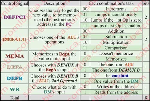
In the table of Figure 11 we summarize the control signals which we can use to talk with our CPU.
There we can verify that those signals are represented by a set of 8 bits, thus 256 possible combinations. But to represent them we only have 4 bits, thus 16 possible combinations.
What about now? With only 4 bits, how will we tell the CPU about the choices and selections it has to do in each situation?
Yeah, but we only want 16 of those 256 possible combinations, our instruction set.
With 4 bits, a decoder is able to select 16 from the 256 possible combinations of 8 bits. This 4 bits set is the opcode (operation code) and it corresponds to one CPU’s operation.
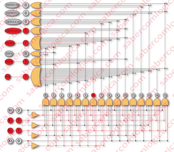
So, we have to introduce a Decoder between the IM and the Control Unit of our CPU in order to convert the operation code provided by the instruction into the control signals which will fulfill the designated task.
In Figure 13 we represent the logic of the decoding circuit for our CPU where we can verify how, with the Opcode 4 selection bits, we can get all the control signals combinations that compose our Instructions Set.
At this point we know how to talk with the CPU in its language. Now we have to create the algorithm with the step by step solution for our problem and translate it into opcodes, which in turn will set the control signals.
Easy, isn’t it? We only have to translate a series of phrases (the steps of the algorithm) into as much lines of 12 digits each (0 and 1) which together will compose the program we want to develop. Well, the only problem is that much probably, as soon as they start to work most of the developers will be completely confused with 0 and 1.
For this reason we’ve set to ourselves a way to replace the opcodes by understandable mnemonics representing them, thereby creating a very low level programming language which is called Assembly.
But thge approach to this or any other form of Programing will come in the next article.
What We’ve Got Till Now
For what we’ve seen until now, it seems that for the CPU, the instruction of a program is a set of control signals sent with its errand boys (bits) through its roads (circuits) to turn on and off the necessary switches (transistors) in order to define the correct path that will take it to fulfill the task that the instruction commanded.
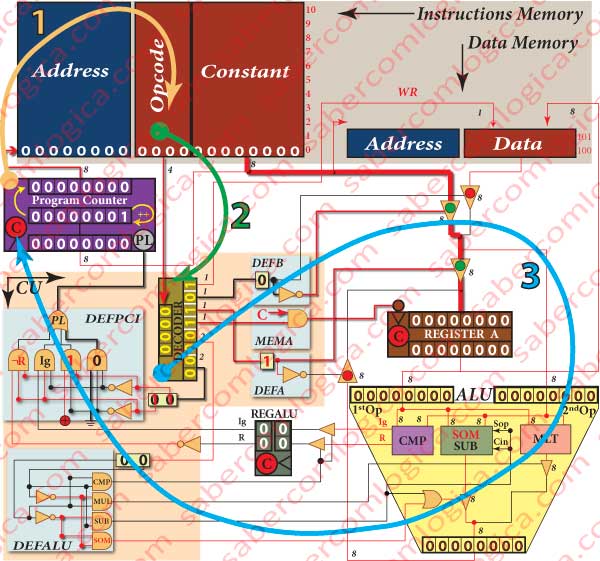
Now it’s time to put together in one only circuit all we’ve defined before. We tried to separate and highlight the Memories, the Control Unit, the ALU and the Registers.
In Figure 1-10 is represented the final layout of our CPU. The thicker lines in Orange (1), Green (2) and Cyan (3) represent the CPU operating cycle:
Fetch, Decode and Execute.