
Logical Gates
The Logical Gates are the transposition, through real electrical circuits of the Computer, built putting transistors together, of the behavior of the logical operators from our mathematical abstraction.
Observation: The resistors inserted into the circuits have the only function of preventing short circuits that burn the transistors when they did not offer any resistance to the electric stream flow .
NOT Gate
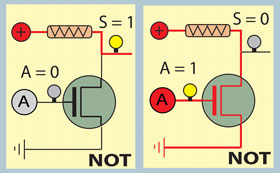
As the solution for this circuit we have one connection line between power and ground, intercepted by a transistor. The electric stream flow between power and ground is controlled by the transistor.
If its gate is subject to voltage (or logic state 1, or lamp A on), the transistor will have a virtually zero impedance, i.e., it will be in the conductive state, thereby providing a preferential path for the electric stream flow. Electric stream always flows through the path with least resistance (the S lamp works like a resistance). Consequently the lamp S stays off, i.e., the output voltage of the circuit is S=0.
If its the gate is not subject to voltage (logic state 0 or lamp A off), it will have an infinite impedance, i.e. it will be in the insulating state. In these circumstances, the electric stream flows through the circuit where lamp S is inserted turning it on, meaning that the output voltage of the circuit is in S=1.
Thus we can construct the truth table of this circuit. If we fill the table values according to the status of the lamp, i.e. on or off, then replacing those words by their meaning, the logic states 1 or 0, we find that the resulting table corresponds to the NOT logical operator.
Thus we can conclude that the action we imagined in the abstract for the NOT operator can be materialized through an electrical circuit that reproduces its behavior.
The Boolean algebraic expression for the circuit is:
NOT A or ¬A
NAND Gate
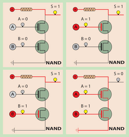
As the solution for this circuit we have one connection line between power and ground with two transistors intersecting it in a serial manner.
If anyone or both of them has not voltage applied to its gate, the electric stream will not flow, thus going through lamp S which is turned on. This means that if A or B or both A and B are 0 then S will be 1.
If both of them has voltage applied to its gate, the electric stream will flow through them, thus lamp S staying off. This means that if A and B are 1 then S will be 0.
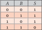
The truth table of this circuit can then be built with the values of A, B and S that we have just mentioned. Compared with the truth table of the logical operator NAND we conclude that the action we imagined in the abstract to it can be materialized through an electrical circuit that reproduces its behavior.
The circuit’s Boolean algebraic expression, starting from the operators expression, will be
A NAND B = NOT(A AND B) or ¬(A.B)
NOR Gate
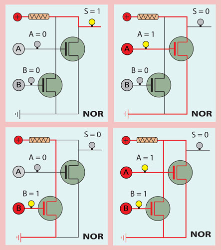
As the solution for this circuit we can see two parallel lines between power and ground, each one intersected by a transistor, thus both placed in a parallel manner between power and ground.
If anyone or both of them has voltage applied to its gate, the electric stream will flow through it, thus lamp S staying off. This means that if A or B or both A and B are 1 then S will be 0.
If anyone or both of them have not voltage applied to its gates, the electric stream will not flow through any of them, thus going through lamp S which is turned on. This means that if A and B are 0 then S will be 1.
The truth table of this circuit can then be built with the values of A, B and S that we have just mentioned. Compared with the truth table of the logical operator NOR, we conclude that the action we imagined in the abstract to it, can be materialized through an electrical circuit that reproduces its behavior.
The circuit’s Boolean algebraic expression, starting from the operators expression, will be
A NOR B = NOT (A OR B) or ¬(A+B)
Introduction to the Remaining Logic Gates
What about if we told you that with this three elementary circuits NOT, NAND and NOR (one transistor, two transistors in series and two transistors in parallel) we have everything we need to realize all the circuits of the computer?
You can only be kidding with us! A computer? That highly elaborated machine? From which we are increasingly dependent for our daily activities? Which manages almost all automations that we experience during the day? No, it can not be true!
But it’s true. In fact, that machine actually highly complex, integrating circuits of tremendous complexity, is composed by the combination of elements of elementary simplicity.
Now we just need to combine those elements of elementary simplicity in successive interconnections that can lead us to the more complex calculation circuits that integrate the latest generation processors.
To understand this we just have to slowly evolve. It can take a long time to get there. But if we are always careful to understand the essence of each step, that is, not only what it does but why it does it, we get there.
Let’s go to another stage in which the output of one logic gate can be the input of another logic gate, thereby obtaining sequential logic operations with elementary circuits.
In terms of abstract logic analysis, we analyzed first the AND operator and then the NAND operator as a derivative, its negation. Likewise we first analyzed the OR operator and then the NOR operator its derivative, also its negation.
Actually, in Boolean logic there are three fundamental operators: NOT, AND and OR. From these came all the others. And in terms of logical analysis remains true.
But in terms of electric circuits we need to do differently, because of the simplicity of the circuits that represent NAND and NOR, leaving these to obtain the others.
You must always look at the NOT operator as an inverter. It turns off what comes on and on what comes off. It turns true to false and false to true, 0 in 1 and 1 in 0.
We will continue to introduce Boolean algebraic expression for each circuit, but always as a result of the solution obtained by logical reasoning.
AND Gate
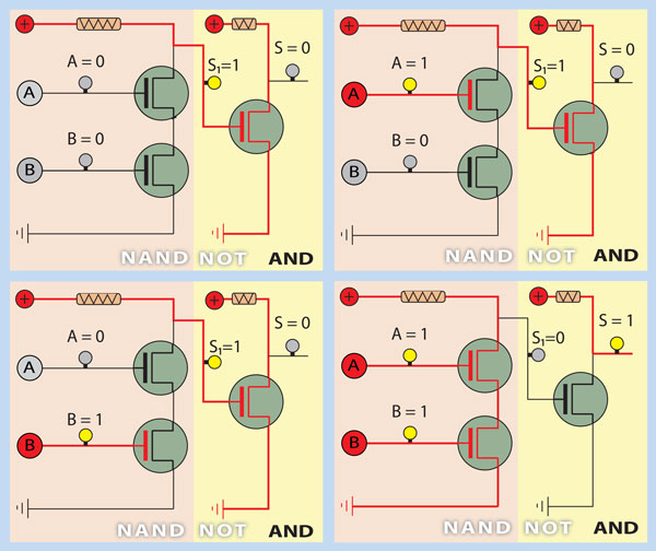
Through the analysis of the circuit, where we still illustrate the 4 possible combinations for the inputs A and B, we can verify that it is composed by the combination of a NAND circuit with a NOT circuit. The denial of the denial of something it’s its assertion.
If we build the circuits truth table by analyzing the transistors behavior according to the evolution of the values in their gates and compare it with the truth table of the logical operator, we can state that this circuit materializes the AND operator.
Using the same symbology, we denote the following equivalence between the algebraic expression of the logical operator and the electrical circuit who materializes it.
A AND B or A.B = NOT (A NAND B) = NOT (NOT (A AND B)) or ¬(¬(A.B))
OR Gate
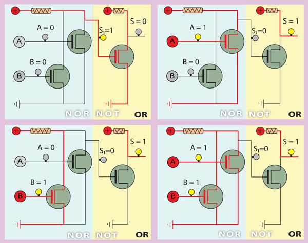
Through the analysis of circuit, where we still represent the 4 possible combinations for the inputs A and B, we can verify that it is composed by the combination of a NOR circuit with a NOT circuit.
If we build the circuit’s truth table by analyzing the transistors behavior according to the evolution of the values in their gates and compare it with the truth table of the logical operator, we can state that this circuit materializes the OR operator.
The circuit’s Boolean algebraic expression, highlighting the equivalence between the algebraic expression of the basic logical operators and the electrical circuit who materializes it, will be
A OR B or A+B = NOT (A NOR B) = NOT (NOT (A OR B)) or ¬(¬(A+B))
XOR Gate
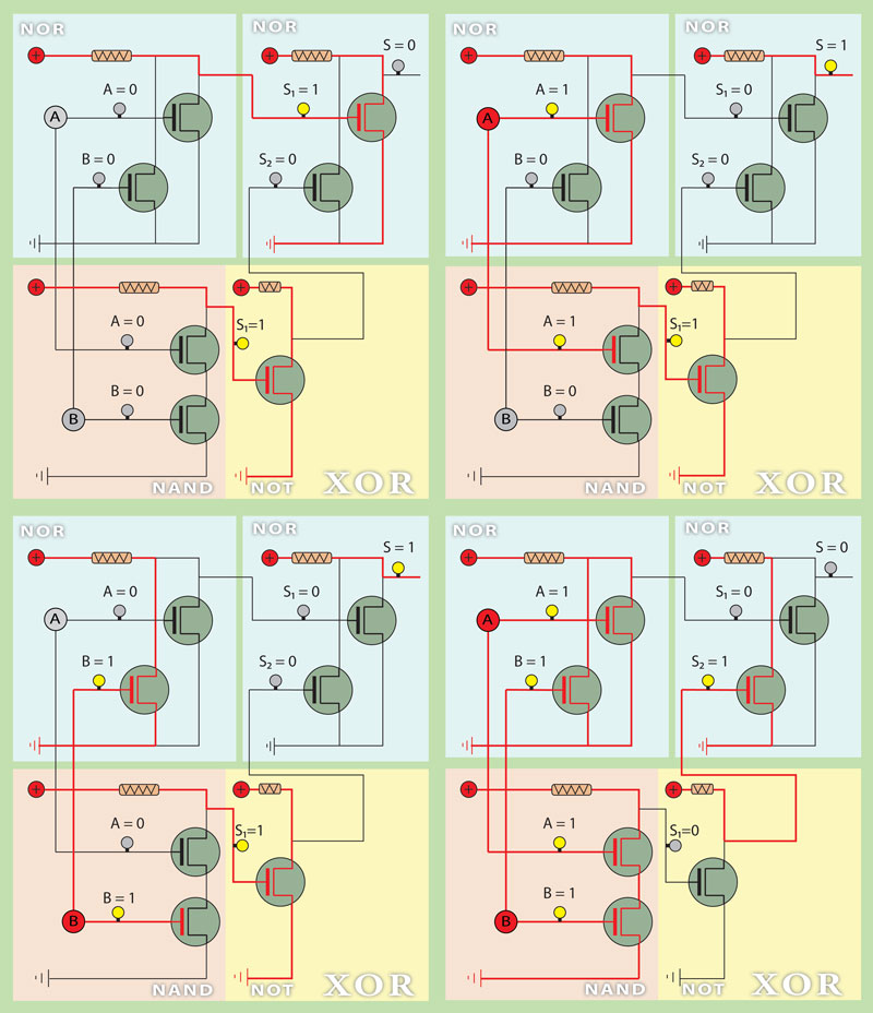
Now we are going to use a good lot of logical reasoning to combine the logical gates that we already know in order to get this new one.
We just have to think about what we want to achieve and hence what values do we need to have at the circuit’s output for the different combinations of the circuit’s inputs A and B.
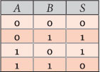
Let’s start with XOR truth table in Figure 11. As we can see, S only is true when A and B are different. None of the gates we’ve analyzed until now as such similar behavior for the possible combinations of A and B.
In order to use the gates we already know to solve this problem, the combination of A and B that will be at the inputs of any gate we know as to be different. Thus, we’ll have to previously work A and B in other gates, in order that those gates’s outputs have the necessary combination for our purpose.
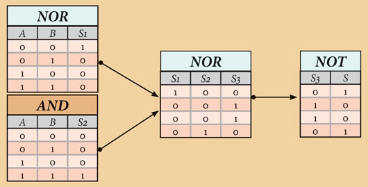
Let’s try it using a NOR gate at the circuit’s output. NOR returns true (1) only when both its inputs are false (0). We are going to call to this NOR gate’s inputs S1 and S2. So, in order we can get our result, S1 and S2 must be both 0 when A and B are
different and both 1 when A and B are equal.
In other words, S1 and S2 must assume the combinations 10,00,00,01 [S1(1,0,0,0) and S2(0,0,0,1)] matching respectively the combinations 00,01,10,11 from A and B [A(0,0,1,1) and B(0,1,0,1)].
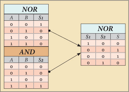
Let’s see it, verifying the evolution through the composing truth tables of the different gates combined as we just have seen, giving XOR truth table, as we can see in Figure 12:
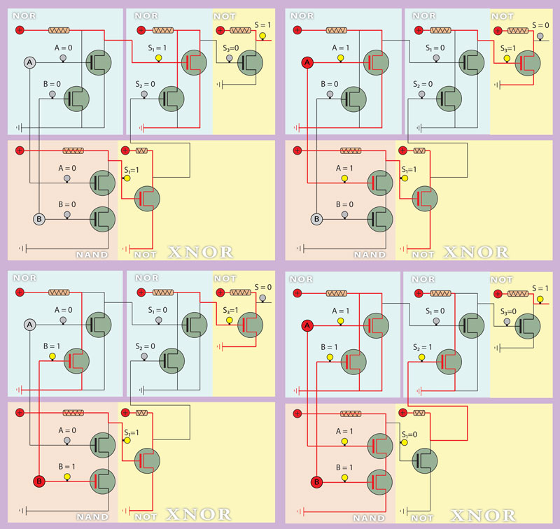
One NOR gate returns exactly the value of S1 in its output for A and B input’s combinations AB→S1=(00→1, 01→0, 10→0 and 11→0).
One AND gate returns exactly the value of S2 in its output for A and B input’s combinations AB→S2=(00→0, 01→0, 10→0 and 11→1).
Thus, what we have to do is to connect A and B to the inputs of two AND and NOR gates and their outputs to the inputs of another NOR gate, which in turn will return the values we want for the possible combinations of A and B.
We’ve got the solution. Let’s verify it in the circuit rebuilding the truth table according to the evolution of the values in the transistors gates.
The circuit represented, shows the electrical circuit matching the intended gates combination, decomposed in the essential gates NOT, NAND and NOR.
The circuit’s Boolean algebraic expression, highlighting the equivalence between the algebraic expression of the basic logical operators and the electrical circuit who materializes it, will be
A XOR B ou A⊕B = (A NOR B) NOR (A AND B) = NOT (NOT (A OR B) OR (A AND B)) ou ¬(¬(A+B)+(A.B))
In order to get to this solution we have defined step by step all the operations to be executed, i.e. we decomposed the global operation in its most essential components. In other words, we defined the problem’s ALGORITHM.
Algorithm? What’s that?
Algorithm
An algorithm is the description of the necessary steps to perform an operation, in the most possible decomposed fashion. For instance, a cooking recipe is an algorithm.
Technically, an algorithm is a finite sequence of instructions defined and unambiguous, each of which can be performed mechanically in a finite period of time and a finite amount of effort.
An algorithm, doesn’t necessarily represent a computer program, but the steps needed to accomplish a task. And its implementation may be performed by a computer or even by a human. A properly executed algorithm will not solve a problem if incorrectly implemented or if it is not appropriate for the problem. For example, an algorithm that describes how we dress ourselves can specify:
“First dress the socks, then put on the shoes, then dress the pants and finally dress the shirt”,
While another algorithm for the same purpose can specify:
“First dress the shirt, then dress the pants, then dress the socks and finally put on the shoes.”
Obviously, the first algorithm leads to a result much less effective and accurate than the second one, even though both lead to the same result.
Why such a long reference to an algorithm?
Because it will be widely used throughout this work. Any logical reasoning should start by creating an algorithm that defines the most basic steps (not decomposable) of that reasoning. The algorithms do not necessarily have to be written. But they should always be part of the mental organization’s process which leads to deductions following a logical reasoning. As is clear, a computer program is essentially an algorithm that tells the computer the most elementary steps to perform a task and in what order they should be executed. As the computer is a simple basic machine this algorithm has to be decomposed to the smallest steps.
For any computational process the algorithm must be strictly defined, specifying its behavior under all circumstances.
XNOR Gate
This purpose can be achieved by a reasoning process identical to the one we followed for the XOR operator, which would result in a solution different from the one presented. To not turn this work louder we are going to use the most elementary way to get there, applying a NOT gate to the XOR circuit’s output, thus inverting it, as we can see in the circuit of the Figure above.
The truth is precisely where both propositions are true or false, that is, coincident. Hence its name of coincidence operator.
Here together goes the truth table obtained from the combination of the involved gates truth tables.
Through the analysis of the transistors behavior for the different combinations of the inputs A and B, which we can see reflected in the final global truth table of Figure 15 we can conclude that this circuit behavior reflects the one of the XOR operator, thus materializing it.
The circuit’s Boolean algebraic expression, starting from the operators expression, will be
A XNOR B or A≡B = NOT ((A NOR B) NOR (A AND B)) = NOT (NOT (NOT (A OR B) OR (A AND B))) or ¬(¬(¬(A+B)+(A.B)))
We leave to each one the reasoning which leads to the determination of the algorithm for a different solution for this problem.
Try to use a NAND gate for the final output.
Tristate Gate
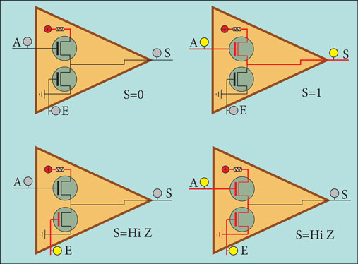
We will represent the electrical circuits for these gates active at the state of 0. So, when the gate is active and E is 0, he information 0 or 1 from A goes to S . When E is 1, nothing happens.
We can see in the represented circuit, the way how E (Enable), activating the transistor whose gate it is connected to, absorbs any value connected to the input A,acting like a switch and respecting this gate truth table.
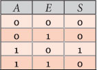
We put here together the truth table resulting from the analysis of the transistors behavior according to the values of the different combinations of the inputs A and E.