Memorizing circuits
The Flip-Flop SR, the Latch D and the Edge Triggered Latch are memorizing circuits which retain bits values in several manners that we are going to analyze in this article.
Flip-Flop SR or Latch SR
The Flip-Flop SR or Latch SR (Set/Reset) is a logical circuit able to be used for memorizing one bit.
We are going to use an analogy to illustrate how this circuit works. For that, we are going to use the door of a room with a lock, containing a latch and a knob.
To close the door, by activating the lock latch, we just have to push it. And it will stay closed if you keep pushing it or even if you stop pushing it entirely. The door assumed the closed state and will stay like that until we act differently in another place, concretely, by pulling the knob, thus deactivating the lock latch and opening the door.
Once the door opens, even if you keep pulling the knob, it will remain open. The door changed its state and assumed the open state. To close it, we will have to act differently and in another place, for example, we’ll have to push it.
We are in the presence of two different actions: push the door and pull by the door knob. The first one closes the door when it’s opened and the second opens the door when it’s closed.
The door only changes its state when the action which changes its state is executed. Notice that not executing any action keeps the door in its present state. Executing both actions simultaneously will put the door in an undefined state, depending on the strengths of the one who tries to open it and the one who tries to close it. Normally the stronger will win, or most likely, the door will be damaged.
Well, let’s leave our door in peace and in its open state so that we can see to the outside, and let’s start analyzing our circuit, which can be seen in Figures 1 or 2.
The Flip-Flop SR can be built with both two NOR (Figure 1) or two NAND (Figure 2) gates, each one having peculiarities in their behavior. Each gate output is connected to the one of the inputs of the other gate. The Flip Flop SR is a Sequential Circuit. The gates communicate to each other their state, thus influencing each other own state.
The remaining input of each gate is where the Flip-Flop SR A and B inputs are connected. When we refer to the output S of a Flip-Flop SR, it is about its upper output that we are referring to. The lower one will always have the first one negated value (¬S).
The actions of pushing and pulling the door, in this circuit, correspond to the SET and RESET actions, giving meaning to the acronym SR.
The input A assumes the SET role. When it assumes the value 1 (push the door), it sets the circuit output to 1 (closing the door), thus setting the circuit. The input B assumes the RESET role. When it assumes the value 1 (pull the door by the knob) it sets the circuit output to 0 (opening the door) thus resetting it.
To understand the operation of a Flip-Flop SR, we will follow its evolution for different values of inputs and for both cases of being built with NOR and NAND gates, as shown in Figures 1 and 2 respectively.

The possible input combinations in a Flip Flop SR with NOR gates are (Figure 1):
- A=1 and B=0, as in Frame I, where a SET is made to the circuit.
- A=0 and B=1, as in Frame III, where a RESET is made to the circuit.
- A=0 and B=0, as in Frames II and IV, where we can verify that, in a NOR gate Flip-Flop SR circuit, not acting in any input won’t change its state either after a SET or a RESET.
- A=1 and B=1, as in Frame V, is a hybrid combination that must be avoided. It sets both outputs to the value 0. Not forcing one output to be the denial of the other gives the circuit an unpredictable behavior.

The possible input combinations in a Flip Flop SR with NAND gates are (Figure 2):
- A=1 and B=0, as in Frame I, where a SET is made to the circuit.
- A=0 and B=1, as in Frame III, where a RESET is made to the circuit.
- A=1 and B=1, as in Frames II and IV, where we can verify that, in a NAND gate Flip-Flop SR circuit, not acting in any input won’t change its state either after a SET or a RESET.
- A=0 and B=0, as in Frame V, is a hybrid combination that must be avoided. It sets both outputs to the value 1. Not forcing one output to be the denial of the other gives the circuit an unpredictable behavior.
The behavior of both Flip Flop SR, with either NAND or NOR gates, is identical in both situations of SET and RESET.
Their behavior will only be different in the situations where both A and B are equal. So, the chosen Flip Flop SR to use must be the one where that situation won’t affect the circuit behavior.
Another verification that we can do regarding the evolution frames is that the circuit state only changes when the variable that can change it assumes the value 1. After a SET the change of A doesn’t affect it. Only the change of B to 1 does. After a RESET, the change of B doesn’t affect it. Only the change of A to 1 will.
This circuit allows us to convert an instantaneous pulse (ex. the clock signal) into a continuous signal, only changeable by another pulse in the opposite gate. It’s like the switch at home. When we push one of its sides (send a pulse to one of the gates) we turn the light on, which will remain on until we push the other side of the switch (send a pulse to the other gate), thus turning it off.
We are going to spare ourselves from an exhaustive explanation of its operational procedure, given that the set of graphical representations that we have presented thus far, together with the knowledge already acquired up to this moment, about the behavior of logical gates, should allow you to take your own conclusions.
Let us then more on onto other subjects.
Flip-flop or Latch D
A Flip Flop SR (FFSR) is able to memorize a value between 0 and 1 in its output, but in order to do that, it needs two variables providing two separate signals, which enables it to change state.
A Latch D, whose composition is supported by the FFSR, is able to memorize in its output S a value D at its input, through the clock influence C.

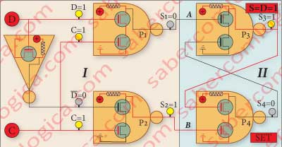
In Figure 3, we separated the Latch in two: part I featuring an FFSR and part II featuring a previous circuit, whose function is to place on the FFSR inputs A and B, values that will make it return what we desire.
In order to do this, the logical gates P1 and P2 from the previous circuit are connected to the FFSR inputs A and B.
And what do we desire?
To have the value D of the Latch input, in its output S, through the use of the clock action C.
And that’s just what the previous circuit does:
- When C and D both have the value 1, the gate P1 returns 0 (B=0) and the gate P2 returns 1 (A=1). Under these conditions the FFSR SET happens, and the value 1, the same value of D, is set at the output S of the Latch.
- When C has the value 1 and D the value 0, the gate P1 returns 1 (B=1) and the gate P2 returns 0 (A=0). Under these conditions, the FFSR RESET happens, and the value 0, the same value of D, is set at the output S of the Latch.
Therefore, the previous circuit, together with the FFSR, makes the latch react as intended to the action C.
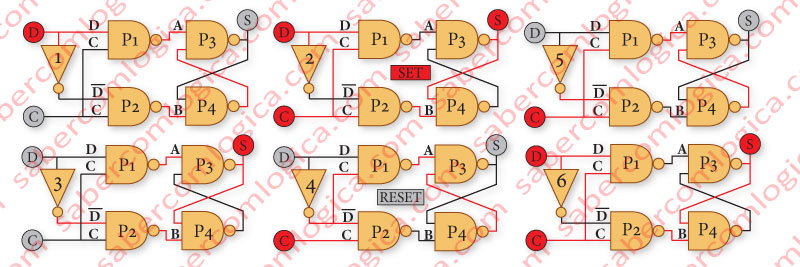
In Figure 4 we can see the latch behavior for several variations of C and D.

In Frames 1 and 3 we can verify that with C at 0, the previous circuit returns 1 at A and B, for every state of D. The two inputs at 1 in an FFSR NAND do not alter its state. Therefore, with the clock at low (C=0), the latch doesn’t react to any changes of D.
In the transitions from Frames 1→2 and 3→4, we can verify that, when C is 1, the gates where D or ¬D are 0, returns 1, thus making the FFSR SET for D=1 and its RESET for D=0. Therefore, when C goes from 0→1 the value of D at the Latch output S is set to that of its input.
In the transitions from Frames 2→5 and 4→6 we can verify that any change in the value of D, changes the value of the gates P1 and P2, consequently turning a SET into a RESET and vice versa, thereby changing the Latch output value to the new value of D. Therefore, while C is high (C=1) the Latch sets at its output S, any modification of its input D.
Edge Triggered Latch D
The Edge Triggered Latch D (ETL), much like the Latch D, is able to memorize an input value D, at its input, through the clock influence C, only it does it by supplying a deficiency of the Latch. The one we described in the last verification.
While the Latch is transparent, meaning that it allows the value S to change when the value of D changes within the same clock cycle while it is high, the ETL won’t change the value of S if the value of D changes within the same clock cycle.
The ETL is not transparent. The value D only set at its output S at the rising edge of the clock (C goes 0→1), or at the falling edge of the clock (C goes 1→0). They can be sensitive to any of the clock edges.
The ETL are the Inns we talked about in Clocked Logic paragraph. When the bits are sent to collect the letters of the word they have to transmit, each one has as a different task. Some of them just leave this Inn and go right on to the next one. Others will have to visit several villages to get the letter they want and only after that, will they reach the next Inn. But the word will only make sense when all the letters are read together. Therefore, the fastest bit will have to wait for the others.
This is where the Innkeeper uses its honors. He lets all arriving bits get in, but only at sunset or at sunrise, will let them go out the exit door.
If these Inns were not spread out along the roads, our bits would always be in an aimless movement, without benchmarks where to meet and get their letters together.
Until the next working period begins, they will have to get to the next Inn, or risk damaging the work of the others in the group because the word will be unreadable without all the letters.
Let’s leave the Inns and come back to the ETL (Edge Triggered Latches), the Inns of the computer. These ETL, together with clocked logic, allow the synchronization of the 8, 16, 32 or 64 bit groups activity. Not allowing any change in the input value while the clock is at high (C=1) will affect the output S, which the Latch D can’t ensure, makes the ETL the perfect tool for the synchronization of all information circulating within the computer circuitry.
The ETL were precisely the tools provided to the CPU for it with the help of Clocked Logic to organize and synchronize the information, in order that, at any given moment, the several circuits of the computer can freeze a specific bit pattern and process it.
Now we’ll use some graphic representations in order to help us prove that the ETL behavior is the one we want. We will confirm that, by verifying the behavior of the output S, when facing the evolutions of the input value D, and of the clock value C, in Figures 5 and 6.
Clock Rising Edge Triggered Latch
By the same analogy, this ETL is the Inn where the Innkeeper only gave access to the exit at sunrise. The guests can get in at any moment, but they’ll keep waiting for the remaining members of the group. Only when the sun rises can they exit the room, showing the letters they’ve brought, in order for the word to be read, and leave on a new mission.
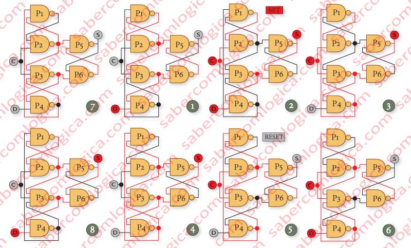
The Clock Rising ETL is built with 3 FFSR NAND [(P1/P2), (P3/P4) and (P5/P6)] interconnected, as shown in Figure 5.

Evolution from Frames 1→2 and 4→5 – C goes from 0→1 when D=1 and S=0, or when D=0 and S=1. The evolution of C from 0→1 represents the rising edge of the clock. The value D will always be set by the output S, which changes.
Evolution from Frames 2→3, 3→2, 5→6 and 6→5– C is high (1), D goes from 1→0 or from 0→1 and S value keeps unchanged, whether it is 0 or 1. We can verify that, when the clock is high (1), changes to D are not reflected in the output S, which remains unchanged.
Evolution from Frames 3→4 and 6→1 – C goes from 1→0 when D=0 and S=1 or D=1 and S=0. The evolution of C from 1→0 represents the falling edge of the clock. The value is never reflected in its output S, which remains unchanged.
Evolution from Frames 1→7,7→1,4→8 and 8→4– C is low (0), D goes from 1→0 or from 0→1. With the clock low (0) any change in D is never reflected in S.
We could verify that, for this ETL, any change to the value of its input D is only reflected in its output S value during the rising edge of the clock C.
Clock Falling Edge Triggered Latch
By analogy, this ETL is the Inn where the Innkeeper only gave access to the exit at sunset. The guests can get in at any moment, but they’ll keep waiting by the remaining members of the group. Only when the Sun sets, can they go out the exit door, delivering the letters they brought in order to complete the word, and leave for a new mission.
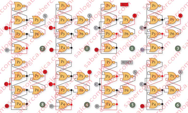
The Clock Falling ETL is built with 3 FFSR NOR [(P1/P2), (P3/P4) and (P5/P6)] interconnected as we can see in Figure 6.

Evolution from Frames 1→2 and 4→5 – C goes from 1→0 when D=0 and S=1 or D=1 and S=0. The evolution of C from 1→0 represents the falling edge of the clock. The value D will always be set by the output S, which changes.
Evolution from Frames 2→3, 3→2, 5→6 and 6→5– C is low (0), D goes from 1→0 or from 0→1. With the clock low (0) any change in D is never reflected in S
Evolution from Frames 3→4 and 6→1 – C goes from de 0→1 when D=1 and S=0 or when D=0 and S=1. The evolution of C from 0→1 represents the rising edge of the clock. The value is never reflected in the output S, which remains unchanged.
Evolution from Frames 1→7,7→1,4→8 and 8→4 C is high (1), D goes from 1→0 or from 0→1 and S value keeps unchanged, whether it is 0 or 1. We can verify that when the clock is high (1), changes to the value D are not reflected in the output S, which remains unchanged. .
We could verify that, for this ETL, any change in its input value D is value reflected in its output S during the falling edge of the clock C.
Registers
Registers are sets of Edge Triggered Latches (ETL) working together with the groups of bits that we have been referring to.
The amount of ETL in a Register is related to the width of the CPUs Registers, the internal temporary memories of a CPU. They will have 8, 16, 32 or 64 ETL each if the CPU has 8, 16, 32 or 64 bits of processing ability, respectively. It’s this width that defines the number of ETL to be placed in the CPU circuitry, for all the Registers.
According to the ETL they integrate, they can be Clocks Rising Edge sensible Registers or Clocks Falling Edge sensible Registers.
Initialization of a Register
Sometimes we’ll have to force all outputs of a Register to either 0 or 1.
NAND ETL Registers
You can follow this description in the two most left graphics of Figure 7 left.

The signals CL and PR will be active at 0.
Why 0?
Both signals will be inactive during the normal operation of the ETL. NAND gates return 1, only if all its inputs are 1. So, CL and PR being 1 won’t interfere with the decision, which will them be dependent on the other inputs alone.
To force a CLEAR of a NAND ETL, we introduce a CL signal to the gates P2/P4/P6. When CL is 0, it forces all these gates to 1, which is actually a RESET to all the FFSR, or to the ETL, whose output will then be set to 0.
To force a PRESET of a NAND ETL, we introduce a CL signal to the gates P1/P3/P5. When CL is 0 it forces all these gates to 1, which is actually a SET to all the FFSR, or to the ETL, whose output will then be set to 1.
Why would we feed this signal to the input of all three gates?
Because we want a stable situation, without the risk of introducing a malfunction to the ETL, after the signal is deactivated.
NOR ETL Registers
You can follow this description in the two most right graphics of Figure 7 right.
The signals CL and PR will be active at 1.
Why 1?
Both signals will be inactive during the normal operation of the ETL. NOR gates return 0, only if all of its inputs are 0. So, CL and PR being 0 won’t interfere with the decision, which will them be dependent on the other inputs alone.
To force a CLEAR of a NOR ETL, we introduce a CL signal to the gates P1/P3/P5. When CL is 1, it forces these gates to be 1, which is actually a RESET to all the FFSR, or to the ETL, whose output will then be set to 0.
To force a PRESET to a NOR ETL, we introduce the CL signal to the gates P2/P4/P6. When CL is 1, it forces these gates to be 1, which is actually a SET to all the FFSR, or to the ETL, whose output will then be set to 1.
