
Motherboard Components
Socket for the CPU
Motherboards incorporate a Socket for the CPU chip. This is one of the components that contributes in large-scale to the non-adaptability of motherboards to certain stages of evolution of computers.
Indeed, both the method of fitting as especially the number of pins of the CPU chips are subject to constant changes, actually resulting from their evolution rather than from trade issues.
For better understanding, it is important to define what are the pins on a chip. The pins are the connection points of the circuits of the CPU with the lines of the Motherboard. The distance between the pins is subject to electrical codes, so that the dimension of the chip package depends essentially on the number of pins. The Chip itself, has a diminished dimension towards its encapsulation.
Let’s try to understand the difference between different CPU chip encapsulations. Just to go not further back, we must remember that a 486 CPU chip had 168 pins, the Athlon 64 FX CPU chip has 940 pins and CPU Core i7 chip flagship has 1366 pins.
In order to realize how difficult it is the compatibility between the CPU sockets for chips, we must take note that within the same family of the latest processors from Intel Core i7, we have the 900 series with 1366 pins and series below with 1156 pins.
Within the same CPU, with the aggravating circumstance of being a modern design from the same manufacturer, how to understand this incompatibility without being through the commercial side?
It is simple. We just have to acknowledge that the 900 series CPU has 3 channels for RAM memory access, while the lower grades have only 2 channel for the same purpose.
A few years ago we had the AMD CPU with independent access to the Main Memory, and Intel CPU chips still placing the whole flow of information through the FSB, so generating a huge difference between both number of pins.
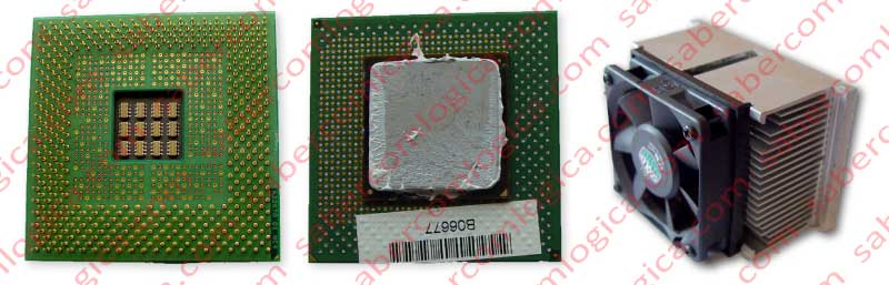
In Figure 1 we can see the photography of a Pentium 4 chip, with the catch pins in sight (left), already embedded in the motherboard and covered with a special white ointment to establish thermal contact with the ventilated sink (the center) and the ventilated sink that will cause cooling (right). This equipment is specific to the motherboard we are examining.
Chipset
As the name suggests, the Chipset is a set of chips, known as Northbridge and Southbridge. These names come from the graphical representation of the Motherboard, which shows the CPU in the top, ie the North, by analogy with the representation of geographical maps. So, the chip that is next to the CPU is the Northbridge and the one who is below it is the Southbridge.
It’s the chipset that defines the CPU that the motherboard supports. Due to the utter incompatibility between AMD and Intel processors, the Chipset solely defines which CPU are supported within one brand and the operation frequency range of the supported CPU.
The Chipset also defines the amount of RAM supported (when the Memory Controller is in the Northbridge), as well as the number of slots to plug-in memory modules. Likewise defines the type of expansion bus supported, according to those that are inserted in the motherboard, being responsible for their control, such as PCI, AGP, IDE, ATA, SATA, PCIe, USB, IEEE 1394 (FireWyre) etc.
It’s in the Chipset that resides the control for DMA (Direct Memory Access), which manages the data transfers directly between peripherals and memory without CPU intervention.
Northbridge
Also known as MCH (Memory Controller Hub) it is responsible for controlling RAM and also for the connection to the bus dedicated to high-performance graphic cards (AGP or PCI Express).
In short, the Northbridge is responsible for the RAM control (for that reason incorporating the Memory Controller), the Hub Link Bus connection with the Southbridge and for the Bus dedicated to video cards. It is also through it and the FSB that the communication is established with the CPU.
Southbridge
Also known as ICH (Input/Output Controller Hub), is connected to the north bridge and its function is basically to control the remaining input and output devices.
It’s to this chip that IDE/PATA bus, in the current case, and more recently the Serial ATA (SATA) bus connect. It’s in this chip that the USB controller resides in conjunction with the Host Hub, which run all the expansions for the various USB ports on the computer.
It’s in this chip that resides the PCI bus controller, 32 bit parallel bus running at the motherboard’s bus frequency through common multiple PCI slots that bind as many daughter boards that will configure, each one, the access to as many devices (SCSI, Sound, Video previously, and many others).
This chip will also control other buses such as PCI Express 1x.
If the Motherboard has audio onboard, the sound controller will also be in this chip. In this case another chip will be available in the motherboard. It’s the audiocodec, inserted between the Input/Output sound and the Southbridge and responsible for encoding and decoding digital sound.
If the motherboard has Ethernet onboard, the controller will also be in this chip. If this is the case, the motherboard should have another chip before connection, dedicated to this communication 10/100/1000 Mbit/s.
Certain connections with peripherals that require much less bandwidth for them to work with much lower transfer rates have been moved to an external to Southbridge chip the chip Super I/O.
Both the Chip Super I/O and BIOS are connected to Southbridge through a bus referred to as LPC (Low Pin Count) characterized for supporting transfer rates lower than the others. We are talking of frequencies in the order of 33 MHz and data transfer rate of 16 MB/s, which are enough to connect the served devices, enabling chips with far fewer pins.
Chip Super I/O
- The Chip Super I/O supports connections with older peripherals such as:
- COM ports (RS 232 serial, e.g.)
- LPT (Parallel – Printer, e.g.)
- Keyboard
- Mouse
- Floppy Drive
BIOS
Ever wondered what a computer does when it’s powered on?
Theoretically anything, because all the information that teaches the CPU to work is in the HDD and our friend doesn’t even know there is one. All the information that was in RAM, the source of the CPU, vanished when it was disconnected. It does less than a lamp which at least gives light for us to see.
So, how is it possible that after we turn the switch on we can have at our disposal all the wonder that a computer provides to us?
Precisely through the BIOS chip and the information it contains.
BIOS (Basic Input/Output System) is a ROM pre-recorded computer program, ran by a computer when it is powered on. It is responsible for supporting basic hardware access, as well as loading the operating system.
Remember the decoders that we talked about in a previous chapter? There, we addressed this issue for the first time, because BIOS is a program written in the form of a mapped instruction decoder, fixed and unchangeable. Hence the term ROM (Read Only Memory). Alternatively PROM (Programmable Read Only Memory) could be used. In PROM, all the connections of the decoder circuit are previously established by fuses which are burned to break the unnecessary links, according to the decoder project, remaining unchangeable thereafter.
After several other solutions more or less related to the name ROM, nowadays the BIOS is recorded in Flash memory.
BIOS works in conjunction with two other programs called SETUP (used to configure some parameters of BIOS), and POST (Power On Self Test) consisting of a sequence of tests made to computer hardware in order to verify that the system is operational.
SETUP information is stored in a tiny RAM built with Flash technology, so non volatile and inserted in Southbridge. It stores information about the hardware configuration, which can be changed when the system boots precisely through the BIOS Setup. This information is used by the BIOS to modify or supplement its default programming as needed.
This little memory was for many years associated with the term CMOS, for this has been the transistor’s technology associated with the Integrated Circuit that contained it. CMOS transistors ultra low energy consumption allowed them to maintain the recorded values for years by feeding them with a small lithium battery.
After loading the interrupt handlers and the drivers for basic hardware, BIOS transfers to RAM the necessary data for the relationship with the hardware that in the future will be used by the OS. After this, BIOS activates POST. We’ll define these strange names just in a moment.
Then CPU, commanded by POST:
- Performs a series of tests to itself and to POST.
- Sends signals through the system bus of the motherboard, the circuit where all the components are coupled and checks if they are running.
- Tests the video card’s memory and the video signals that control the monitor. The BIOS of the video card becomes part of the total system BIOS and memory configuration.
- Tests the RAM modules chips, writing on each one and then reading each byte who was sent. The comparison between what was sent and stored in memory and what is read is made to ensure that RAM its properly working.
- Checks if the keyboard is properly connected. Scans for mouse properly connected.
- Sends signals to the disks by specific buses. The response to signals indicates which drives are available.
The results obtained in the tests are compared with data recorded in SETUP.
The problems, if any, are communicated by a combination of sounds (beeps) in a particular sequence and if possible, displayed on the monitor. The manufacturer’s manual allows the identification of the problem describing the message that each beep sequence represents.
Then BIOS reads the computer storage systems according to the settings and with the priority order recorded in SETUP.
SETUP allows us to define the order in which the storage devices must be accessed in order to find an OS. Originally it was the Floppy Disk Drive the first to be accessed and, if there was no media inserted in it, then the HDD was accessed.
In case of failure in HDD a friendly message was sent:
- “Boot Failure on Drive C:”
- “Insert Disc on Drive A:”.
Afterwards the Floppy Disk Drive was replaced by CD/DVD Drives. Nowadays any USB bootable source can be chosen as firs access. Better yet, we can define during the boot a different first access source, so allowing HDD to be set as the primary boot device, avoiding the sympathetic message “Boot Failure on Drive X:” when we had forgotten some media inserted in the first access Drive.
Performed these routines, the BIOS loads into memory the boot code from the MBR (Master Boot Record), the first sector of an HDD, which knows of the existence and location of an operating system installed, in order to give it the command of the operations.
This part is much more complex to describe now. We will introduce the terms attached to such a demand, getting the correct description of a computer booting operation to the chapter about File Systems, in which we will talk about the logic of the HDD (Hard Disk Drive).
The booting process will now load the OS. It is sent to RAM and assumes the CPU control.
Now, the information we had promised.
Interrupt handlers are small pieces of software that act as translators between the hardware and the operating system. An example: when a key is pressed, the event associated with the fact is sent to the keyboard interrupt handler, which refers it,translated, to the CPU. CPU treats and sends it to the operating system that disrupts the ongoing process to meet the new request. Something that we will see in more detail when we talk about OS.
Drivers are small pieces of software that identify each piece of hardware to the system, showing you how they can be operated.
Other components
In addition to other buses which might exist in the motherboard but which are not a standard, there are other minor components such as:
RTC
RTC (Real Time Clock),its a little CMOS chip that keeps permanently up-to-date the date time value.
Battery
Keeps RTC running. Formerly also had to keep BIOS SETUP, which now as we have seen, is in flash memory embedded in Southbridge.
Quartz Crystal
This crystal, in conjunction with a suitable electronic circuit, in which is included the PLL (Phase Locked Loop) chip, is the generator of the clock signal of the computer. With the appropriate gear ratios and multiplications it is responsible for the clocking of the entire computer.
Front Panel Computer Connectors
Motherboard includes a 20 pin dock that lets you connect various functions offered by the front panel of a computer case, such as:
- Reset Button
- On/Off switch Button.
- LED activity indicator of HDD.
- Led power indicator On.
- Loudspeaker.
Motherboard Power Connector
Normally, for an ATX board and an ATX power supply, a 20 pin connector provides power to the board voltages 3.3V, 5V and 12V.
Voltage Regulators
The voltage used by components like the motherboard chipset, CPU, expansion bus and others are now so low and diverse that even the most modern power supply is not able to provide it. In order to surpass that lack, there are, welded to the board, several voltage regulators that have the effect of correcting the voltage range for those components.
Capacitors
Their role is filtering the electrical signals that travel through the motherboard. They may go unnoticed but are usually in large quantities.
Fan Connectors
Specifically, CPU, Northbridge and Graphics Card have heat sinks that may or may not have engaged fans, because of their special overheating. Because there are more heat sinks elsewhere in the Motherboard, the PC case must be provided with a fan .
All these fans connect to plugs that for that purpose exist in Motherboard