
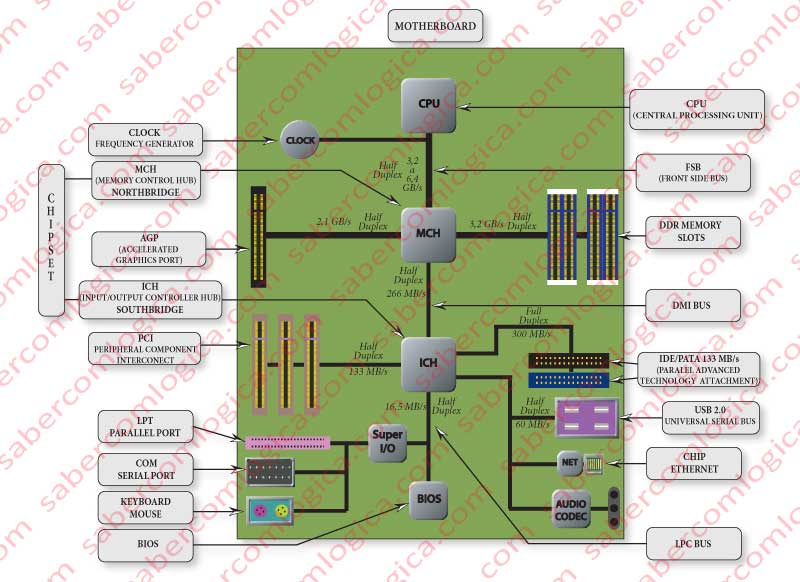
Motherboard Layout and Printed Board
The Motherboard, is a complex printed circuit where the essential computer chips are embedded, along with capacitors, resistors, voltage regulators and others that make the management of all components of the computer.
The main function of a motherboard is to connect CPU with main memory and too with the world that surrounds it, through the device I/O. In order to accomplish that purpose it offers a huge multitude of lines, Plugs, Sockets and Slots.
Every internal or external component connected to the computer, is connected to the motherboard, the only way to be recognized and communicate with CPU. Even if the components are apparently not connected to the computer, operating through infrared communication or radio frequency, they are effectively connected to the motherboard via the appropriate receptor.
Let’s say we have a great city, with buildings where city management systems are installed, and buildings where companies that carry out essential activities around this city are installed. At the top of the hierarchy of this city is the CPU building, around which are the buildings where the CPU unconditional servers (bits) live .
Connecting all these buildings there’s a multitude of roads, some bigger, some smaller and others still authentic highways, through which circulate the couriers that carry information between the various buildings (the bits), commanded by the CPU.
This huge network of roads is the PCB (Printed Circuit Board)on which is built the Motherboard.
Printed Circuit Board
As its name suggests, printed circuit board is a circuit composed of conductor lines (mainly copper) printed on a board of insulating material, such as fiberglass for example.
To build a Printed Circuit Board there are several methods, such as screen printing, and other photographic processes. Let’s talk about the photographic process.
The printed circuit board we will describe is constituted by a glass fiber board coated on both sides with a thin copper foil. As a first step, the board is bathed in a film of photosensitive material resistant to the action of abrasive chemicals, thus remaining the board totally involved by that material. Then the board is subjected to a photolithography process, that consists in exposing it to light passing through a mask corresponding to the design previously developed for the electrical circuit that is intended, on each side of the board. Once exposed to light, the exposed photosensitive material becomes soft and is removed. Thereafter, the board is introduced into a bath of corrosive solution (nitric acid for example), which removes the unprotected copper foil areas (where the photosensitive material was removed).
Thus remain drawn on the glass fiber board the lines of copper circuit. After the removal of the remaining (the not exposed) photosensitive material and the drilling of the board in the places provided for connections, the PCB is ready for the introduction of the components.
To these copper lines printed on the board, we will call Motherboard Buses and, as we will see, they are responsible for better or worse CPU performance.
Let’s realize how is organized a Printed Circuit Board of a Motherboard identical to the one defined in the Layout of Figure 1.
Empty Motherboard Analysis
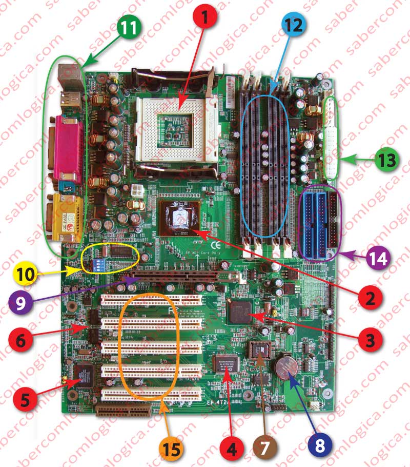
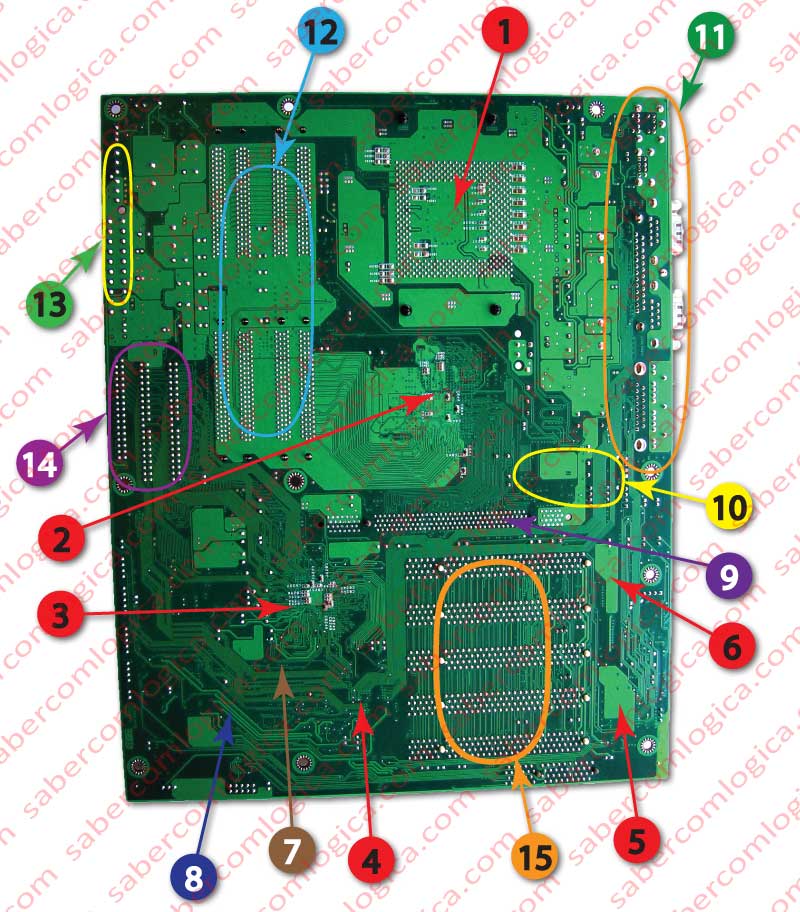
We will start by describing the components of a motherboard used whose architecture was in use for a long time and still exists on many running computers. It has its graphical representation in the context of Figure 1, corresponding to the photographs of Figures 2 and 3 respectively taken at the front and the inside face of a Motherboard with organization similar to the graphic frame.
Its evolution was pushed in order to achieve the increasingly demanding data transfer requests between current processors, RAM memories and graphics cards, image processing.
The Motherboard represented in the photos has the same architecture represented in the graphic of Figure 1. It supports a Pentium 4 @ 1.6 GHz and its construction is from 2001/2002.
We can see some of the components of the graph in its actual location. For its analysis we will use the photography of Figure 2, corresponding to the top of the motherboard and also the photography of Figure 3, corresponding to its back.
In this paragraph it’s our purpose solely describe and reference what’s is visible to the several components. Further on we will analyze each component functions. Thus we have:
- Socket for fitting the CPU.
- Northbridge In the back of the motherboard we can see that the lines of the printed circuit derived from it are directed essentially to the memory slots (Right) and to the AGP (Accelerated Graphics Port) slot for the video card. In the top of the motherboard we can see the lines which connect it with the CPU, known by the name of FSB (Front Side Bus), the BUS between the CPU and all the computer.
- Southbridge In the top of the motherboard we can see the lines connecting this chip to the PCI slots. In the back of the motherboard we can see the lines connecting to the Super I/O Chip, the BIOS and the IDE/PATA plugs.
- Super I/O Chip. The main connections from this chip are seen on the back of the Motherboard. There we can see the lines who connect it to the standard plugs and the lines who connect to the Floppy Disk
- Audio OnBoard control Chip.
- Ports control Chips.
- BIOS
- Lithium Battery.
- AGP slot for video cards.
- Motherboard’s clock. We can see a set of switches which allow to define frequencies, the quartz crystal within a metallic capsule and the chip PLL (Phase Locked Loop) that rectifies the frequency of the quartz crystal and produces the frequencies of the several operating components that connect to the Motherboard. It’s this set that constitutes the Motherboard’s Clock
- Set of plugs for the standard connections embedded in the Motherboard, which will identify further on.
- Slots to plug the RAM memory modules.
- Plugs to power the Motherboard and consequently all components connected to its slots (memory and AGP and PCI cards)
- IDE/PATA connecting plugs, aimed at internal HDD drives, CD/DVD and Floppy.
- PCI slots.
We can see a lot more components connected to the Motherboard, such as resistors, capacitors, frequency brokers, chips and many others, which we will not identify as being outside the scope of what this work proposes.
In the back of the motherboard are evident the welds of the Slots, Plugs and Socket’s contact pins.
Next, we will look at a picture of the same Motherboard filled with the components that enable the connection between the CPU and the world outside it, as we can see in Figure 4.
Filled Motherboard Analysis
The slots, plugs and socket are now already filled and some other elements have been added. We describe the added elements identified by the numbers in Figure 4:
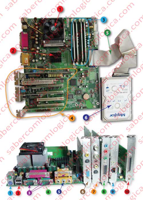
- 1. The CPU was placed on the appropriate socket and over it was placed a ventilated thermal energy sink.
- 2. Over the Northbridge was also placed a heat sink. In the photo of Figure 2 the chip is covered with a white mass, whose aim is to improve the contact between the chip and the heat sink.
- 3. The memory modules have already been placed.
- 4. Several Boards with specific communication with external components, are also placed in the PCI slots.
- 5. An Ultra ATA 80 conductor cable with three connectors: Blue for connection to the system, Black for connection to the Master and gray to connect to Slave. Master and Slave are the names given to primary and secondary hard drives in IDE/PATA, when there is more than one HDD.
- 6. Hard Drive IDE / PATA, ie, an HDD which uses an interface IDE/PATA (Integrated Device Electronics / Parallel Attachment). This standard was current in modern HDD for the Motherboard in question and remained for much longer, at least until the connection ATA, PATA or Parallel now AT Attachment was replaced by SATA or Serial AT Attachment.
Let’s now look to the plug connections of the Motherboard and also those provided by Daughter boards inserted in the slots of the Mother.
The view from the Motherboard’s Left Elevation, which will face the back of the computer box after mounting, being an integral part of it, is where the connections are listed, as we can see in Figure 4 below . Thus we have:
Connections integrated on the Motherboard:
- Jacks for connecting PS2 mouse and keyboard.
- USB plugs.
- Serial ports COM 1 and COM 2.
- Parallel port LPT1.
- Audio inputs and outputs of the audio onboard system, embedded in chips which are part of the board itself.
Connections provided by the Daughter boards:
- Video Card, with VGA, S-Video and composite video plugs.
- Video and TV capture card with FM and TV antenna, phones output, composite video and S-Video plugs.
- Sound Card, with stereo L/R output, phones output and analog joystick plugs.
- Ethernet card for computer connection with networks and Internet, with an RJ45 plug.
- SCSI card for connection to external SCSI standard components.
Now we will analyze the main components of the Motherboard and see how they fit on its corresponding PCB.