Parallel Transmission Buses
FSB (Front Side Bus)
FSB is the set of lines from the motherboard through which CPU communicates with the Northbridge chip and consequently with all computer components. As mentioned earlier, this bus is limiting the frequency of vibration that the set of computer runs. The frequency of the quartz crystal is modulated to the frequency of the Motherboard buses. Above this frequency the lines generate electromagnetic noise that can corrupt the values passed in the nearest lines. This, in addition to time skew, already explained.
Much has been invested in the FSB, to increase the amount of data that pass through it. Increasing the width of the data, i.e., the number of lines thus increasing the number of bits per cycle. Through the Double Data Rate and Quad Data Rate (Intel processors carry 4 sets of data per clock cycle , which is called Quad Pumping). The transfer capability of a bus corresponds to the product of the bandwidth (assume 64 bits), the number of data per cycle (admit 4) and vibration frequency (100 MHz suppose), which in this case corresponds to 3.2 GB/s.
Double data rate
It is obtained sending a bit on each edge of the clock signal, a technique still used in DDR memories.
Quad Data Rate or Quad Pumping
Corresponds to sending a bit on each side of the clock signal and two others at intermediate points.
And how can we get this?
Creating a complementary clock signal from the real and lagged by 90 degrees which also allows sending bits on their ascending and descending edges. This technique was adopted by Intel, which could thereby quadruplicate the throughput of its FSB up to a maximum of 6.4 GB/s.
Memory Bus
The slots for RAM are connected to Northbridge for a dedicated bus. The RAM chips are included in modules that are inserted into slots.
The memory bus can be a normal, doubled or quadded clocked with one bit transfer in each edge of the clock, according to the type of RAM used (from SDRAM to DDR3). This high transfer data rate is possible due to the direct connection to CPU in recent memory computer architectures, i.e., the Memory Controller resides in the CPU Chip.
Because main memory is, along with the processor, one of the major computer components, working closely with CPU, it will be discussed later on several occasions and in several stages, as our knowledge is evolving and accepting concepts of greater complexity .
PCI Bus
The PCI (Peripheral Component Interconect) Bus has replaced almost all types of expansion buses to its existing development.
It was created by Intel and its specifications were published and delivered to an independent PCI-SIG which thereafter developed the successive revisions of the specifications for the PCI. This fact, coupled with the exceptional features of this bus compared to the existing, made it palatable to all hardware manufacturers, what led to a bus that quickly became standard on all motherboards.
The PCI is a 32 bit parallel bus that works in its basic form at a frequency of 33 MHz. The same PCI bus can connect multiple PCI slots.
Slot is the English term for a special type of plug-shaped groove with contacts on both sides, where the printed circuit boards from other components fit via a ledge also with contacts on both sides.
Residing components of the motherboard can also connect themselves through PCI bus. Until the implementation of HL (Hub Link), Intel’s proprietary bus for communication between Northbridge and Southbridge chips (Hubs) was PCI Bus .
Besides those already mentioned, another reason that led to the universal adoption of this type of bus was that it incorporated the standard PnP (Plug and Play). At the launch of this standard nothing was felt, but when a few years after Windows 95 for the first time brought PnP support, the demanding of computers with PCI Bus arose quickly driving down the until then used ISA bus.
The PCI bus connects directly to the Southbridge, which manages the allocation of several components to the line and controls the frequency of the bus clock.
Later we will take a short approach to the standard PnP, where the PCI bus was precursor and which dominates the computers of today.
AGP Bus
The quick evolution of video cards, with the consequent request for greater bus transportation capabilities, led to the creation of another bus called AGP (Accelerated Graphics Port) with performances lot better adapted to the needs of applications for 3D graphics.
AGP was not more than a PCI bus, which differed in two essential characteristics:
- It had a dedicated bus for each AGP (one on each motherboard).
- It was accelerated, as its name suggests, what allowed it, with the same frequency of PCI Bus, to transfer 1, 2, 4, or 8 bits per line in the same clock cycle. This was achieved by the same process already mentioned.
We won’t say more about this bus, because he has already been replaced by PCI Express.
LPC Bus
LPC (Low Pin Count) is used to connect the BIOS and the Super I/O chips to the Southbridge chip. Its main advantage is the simplicity and elementarity resulting from being the support for older and slower peripheral, requiring far fewer connections, and so being easy to route in a motherboard already overloaded with connections. The clock frequency this Bus uses is of 33 MHz, the same as PCI bus. Its transfer rate is typically of 2.56 MB/s.
Serial Transmission Buses
PCIe (PCI express)
Why replacing a technique that transmits 32 bits at a time by another that transmits only one bit at a time?
The serial transmission is performed in a differential way, i.e. by means of two cables, twisted and balanced, that is, with equal impedance along its length and equal impedances with respect to ground and to other circuits, which we will call D+ and D-.
There are several methods of differential transmission. The PCIe method consists in introducing a determined voltage value in one of the cables. AV is the voltage value for the logic state 1 and the value 0V to the logic state 0.
When we want to send a 1 we inject AV in D + and 0V in D-. The reading is done by subtracting the two values and in this case will be AV for D+> D-, corresponding to a logical value 1.
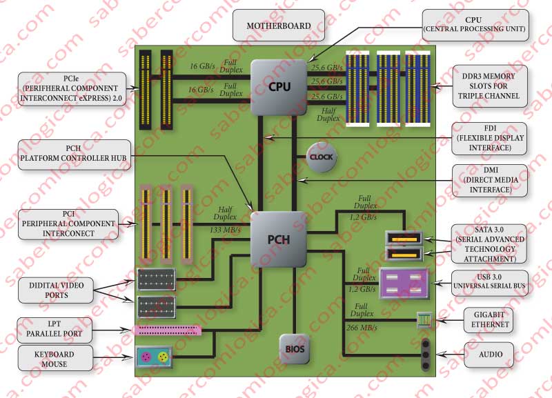
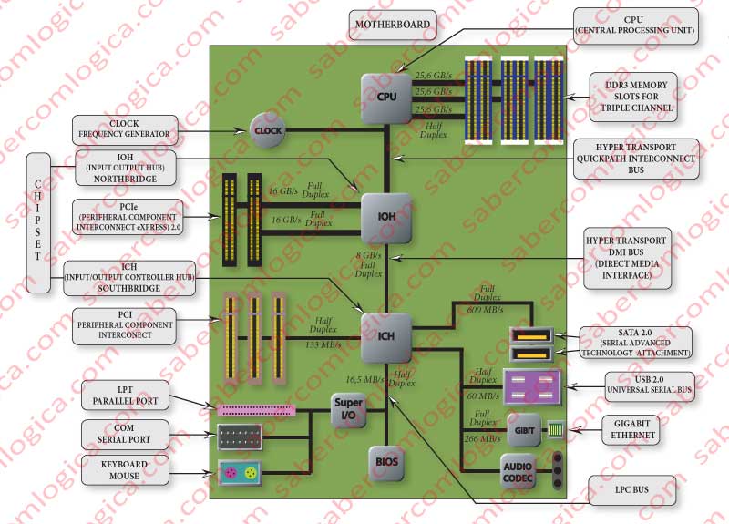
When we want to send a 0, we inject AV in D- and 0V in D + . The reading result of the subtraction of the two values will be -AV, for D+ We will have a difference between the two logic states 0 and 1 equal to AV-(-AV) = 2AV, which substantially reduces noise interference. The noise, if any, will introduce itself in the two cables in the same way and when the subtraction of the two values in the receiver is done it is canceled. In differential transmission what matters is the sign and the voltage difference. We can thus increase the frequency to values which can reach the frequency of CPU. Instead of two cables we have four and consequently an unidirectional transmission in each pair and simultaneously in both directions (Full Duplex) in the two pairs. This set of cables is called Lane and comprises two links. We can add more Lanes up to a total of 32, having possible 1, 2, 4, 8, 16 and 32 Lanes, which give rise to the designations PCIe x1, PCIe x2, PCIe x4, PCIe x8, PCIe x16 and PCIe x32 . PCIe x32 has not yet been put into practice. The transmission PCIe is a point to point transmission, i.e. lines that serve each device are exclusive and not shared. In this first version of the PCIe we can reach transfer rates of 8GB/s. It was in the sequence of these developments that AMD adopted the Hyper Transport Bus as a substitute for FSB. Serial ATA or SATA SATA (Serial Advanced Technology Attachment), is a technology used to transfer data to and from mass storage devices, specifically Hard Disk Drives (HDD) and Optical Drives (CD/DVD/BRD). It corresponds to a further evolution from parallel to serial on the type of buses supporting large volume of transfers and therefore requiring higher transfer rates. Specifically it corresponds to the evolution of ATA (Advanced Technology Attachment) technology, also known as IDE (Integrated Drive Electronics) which was renamed PATA (Parallel ATA) precisely to distinguish it from SATA (Serial ATA). The SATA connectors communicate directly with an AHCI (Advanced Host Controller Interface) that must be resident in the Motherboard Chipset. From there they communicate with the CPU or directly with memory via DMA (Direct Memory Access), normally this last one, once nowadays HDD is accessed by MMS (Memory Management System) for block transfers to RAM. The 2nd generation of SATA, SATA II or SATA 3 Gbit/s as this is its transfer rate, is also found very frequently in many computers, even some on sale, since HDD don’t yet absorb its full bandwidth. The current generation of this technology SATA or SATA III 6 Gb/s, is nowadays implemented in most PC of higher performance currently marketed, as the current Solid State HD (SSH) based on Flash technology, can exceed the capabilities of SATA II. This connection is intended for components connected by cable to the Motherboard, internally to the computer case. The differential serial transmission used in this technology is based in 1 Lane (2 unidirectional links), so Full duplex. The control of the corresponding differential is the same that we will describe to the Hyper Transport bus. USB (Universal Serial Bus) USB is a technology aimed at connecting external peripherals to the computer. The data transmission is done serially, half duplex, ie, in one direction at a time, bit by bit. USB follows the great expansion of personal computers and comes from the need to turn the connection of various peripherals easier. This technology was designed from the viewpoint of the concept Plug and Play (PnP). Before USB came to light, the connections from computers with external peripherals was limited to two serial ports, one parallel port and some PCI expansion slots on the motherboard, which could install signs for specific external connections, such as video, network, sound and others. Installing an external peripheral was usually complicated and requiring the intervention of specialized technicians for it was necessary to define a set of parameters for each component, such as IRQ (Interrupt Request) and maneuver “jumpers” (this was the name of small pins that were used to join two contacts) that came on the boards or peripherals. If something was not properly implemented conflicts were generated that could prevent the peripheral’s operation or even more block the computer. The PnP concept has revolutionized these problems because it turned easy the installation of peripherals by any user with some knowledge and fairly dashing. It was the combination of USB with PnP that made common connecting any components to a computer. USB allows the connection of several components to the computer, starting from a Master Hub existing in Southbridge in sequence of which and in a Tree topology more Hubs can be connected, giving more possible connections, to a maximum of 127 components and a maximum of 7 Hub levels including the Master Hub, also known as HOST. The type of connector is common to all peripherals that use this technology, thus making it easy to design them with respect to the support by the operating systems and hardware. It created a standard that allows the operating system and the motherboard to identify the type of peripheral, its power needs, its bandwidth needs and others, as soon as it is detected and identified. When the computer boots, the USB devices connected to it are detected and are assigned a number. Each time a device is connected to the computer through a USB port and its presence is detected: The controller and the OS verify if they already have its drivers or if they are included in the device itself, and place them in a position to be used. If the device drivers are not available it’s required to the user to enter the disc containing the drivers provided by the manufacturer. More recently, the OS itself queries a database where the vast majority of drivers for that OS is stocked. The most common USB version currently running on computers and mobile devices is 2.0, which allows connections with a transfer rate of 480 Mbits/s (80MB/s) against the 12 Mbits/s (1.5 MB/s) of the previous version 1.1, completely abandoned. On almost every new PC is now the new USB version 3.0, which has transfer rates of 3.2 Gbit/s (400 MB/s) in full duplex, exceeding transfer rates currently achieved by the HDD on the market. BIOS is the core program that enables PnP. It reads the ESCD (Extended System Configuration Data), i.e. in terms that we can understand, it queries a file that has the name ESCD which contains information about the installed PnP devices. An operating system compatible with PnP completes the process started by the BIOS. PnP automates the following tasks: And how does it work? During boot, BIOS identifies all the hardware present and asks each one to identify itself. When it gets it, checks if it already exists in the ESCD. If not, the BIOS assigns him IRQ, DMA, memory address and I/O configuration. And records this data and the device in ESCD. Subsequently the Operating System (OS) queries the ESCD, checks the devices and loads the drivers (small identification programs of the device for that OS) necessary for its recognition or asks their installation from disk provided by the manufacturer, if the respective drivers aren’t yet installed. Currently it is normal that the drivers come included in the device, in a way that they can be read by the OS during its first use. Recently and for questions of security, the OS itself queries a database where it keeps the drivers that each manufacturer gives it when the product is launched in the market, as is the case with Windows 7 and 8, for instance. The drivers are installed in the Kernel of the OS, a sensitive area for the computer security, and the installation of drivers through CD introduced by the user has originate severe security lacks that OS now intend to avoid, proceeding this way. As all the communications between CPU and the remaining components (such as HDD, RAM, Video Card) of the computer had to go through the FSB it became a permanent bottleneck for the constant evolution of processors, memories, video cards and other components. The huge advances made by the video cards supported by PCI Express, allowing data transfers of 8 GB/s maximum, made them alone exceeded the capacity of FSB. Not to mention the permanent access that the CPU has to do to the main memory, in its ongoing increase transfer rates (DRAM, DDR, DDR2, DDR3). There is no doubt that FSB was working as a brake on the growth of new technologies, it did not allow its exploitation beyond values that were becoming insignificant compared to the development of all components. Perhaps because it was the manufacturer with the lowest transfer rates in FSB, AMD was the first to invest in a completely different architecture for data transmission in FSB and layout of organizing buses in Motherboard. The evolution trend of buses is to be, at all levels, the transition from parallel to serial transmission. Serial ATA (SATA) and PCI Express (PCIe) represent evolutions of their predecessors PATA and PCI from parallel to serial transmission. Not to mention USB and Firewire ever born as serial communications which have experienced and continue to experience enormous developments, especially in the field of USB. Hyper Transport technology was adopted by AMD and created by a consortium of AMD, NVidia and Apple. The Hyper Transport bus was implemented by AMD together with the AMD64 architecture. It is a point to point serial transmission sending two bit per clock cycle, in the ascending and descending edges of the clock, and full duplex. Hyper Transport is a bus with Lanes with two links per Lane, one in each direction. The transmission is serial differential, but the method of transmission is different from the described for PCIe. The Hyper Transport bus is conceived for transmission through packets of n words of 32 bit each, regardless of the width of Lanes of the connection. The transmission is always initiated by a word that contains the code of the transmission. The number of bits is always a multiple of 32, regardless of the size of data to transmit. The Hyper Transport bus is aimed to replace the FSB but also for communication between processors in multiprocessor or multicore CPU. Along with Hyper Transport Bus AMD implemented its AMD64 architecture which includes the transfer of the memory controller from Northbridge into the CPU chip, so being the memory access made directly from the CPU chip to the memory modules and through dual channel, also changing the layout of the motherboard, as shown in Figure 1. It’s the Intel version to replace FSB. In all similar to HyperTransport but with no compatibility between the two solutions. It’s a serial transmission, point to point, with two data per clock cycle and Full duplex. It consists of 20 lines and transmission is done in blocks of 80 bits, which are sent in two clock cycles. Of these 80 bits, 8 are for error control, 8 are for link layer header and 64 are for data. Working at a frequency of 3.2 GHz achieves a throughput of 25.6 GB/s in both directions (full duplex). It will also be through this type of bus that cores in multicore CPU interconnect and that multi CPU interconnect too. This bus comes in the wake of a new architecture designed by Intel, Nehalem, which will be discussed in our case studies throughout this work. Communications with the memory were removed and transferred from the Northbridge to CPU chip by embedding the memory controller on the same, so changing the layout of the motherboard to the one in Figure 1. PCH (Platform Controller Hub) results from the dump of Northbridge functions to the CPU chip. After acquiring the memory controller, which gave it a direct link to the memory, it also happened to get PCIe lanes. This way Northbridge was spoiled from its main functions Thus, Southbridge has incorporated all the functions of I/O and control of the remaining features of the motherboard. Beyond those who already were peculiar, it has incorporated the RTC (Real Time Clock), the Super I/O chip functions, the Ethernet chip functions and others, taking the name of PCH (Platform Control Hub), really consistent with its new functions. The PCH chip also has the display controller, as it is its responsibility the communication with the display where the CPU chip has already incorporated the graphics processor and no Video Card is used. This change occurred even with the Nehalem architecture and is supported initially by Intel Atom, Intel Core i3, Intel Core i5 and Intel Core i7 with the exception of 9xx series. The PCH chip has two different communications with the CPU chip: DMI (Direct Media Interface) previously used in communications between Northbridge and Southbridge, which with its DMI 2.0 evolution delivers transfer rates of 20 Gb/s between the CPU and PCH. FDI (Flexible Display Interface) is a link created specifically by Intel to support the connection between the CPU (incorporating HD graphics and GPU) and PCH, solely for the graphic communications. In this case the output video plugs shall be in the motherboard itself. Both DMI and FDI were introduced during the various architecture innovations in Intel Core i7, from Nehalem to Sandybridge and Ivybridge, and with the decreasing size of transistors which in the first i7 was of 45 nm and which is nowadays of 22 nm. Figure 2 attempts to illustrate what will possibly be a current motherboard.Plug and Play (PnP)
FSB Evolution
Hyper Transport Bus
QuickPath Interconnect
PCH