Shifting Registers
Registers are sets of Edge Triggered Latches (ETL) working together with the groups of bits that we have been referring to.
The amount of ETL in a Register is related to the width of the CPU Registers, the internal temporary memories of a CPU. They will have 8, 16, 32 or 64 ETL each if the CPU has 8, 16, 32 or 64 bits of processing ability, respectively. It’s this width that defines the number of ETL to be placed in the CPU circuitry, for all the Registers.
According to the ETL they integrate, they can be Clock Rising Edge sensible Registers or Clock Falling Edge sensible Registers.
Sometimes it is necessary to shift the bits from one register to either the left or to the right.
Specifically, when performing a multiplication and/or division with iterations, with each iteration corresponding to a shift of the operating digit to the left or right. Shifting a number one bit to the left is equivalent to multiplying it by 2. Shifting a number one bit to the right is equivalent to dividing it by 2.
A common use of Shift Registers is the conversion of parallel streams (one complete bus, ex. 8 bits, at the same time) to serial transmission (one by one). The 8 bits are fed to the outputs of the shift register and a set of eight shifts is initiated. For each shift, one bit goes out to the serial transmission line. When finished, a new set of 8 bits is fed to the outputs of the Shift Register, and a new conversion begins. The same thing applies to the reverse process.
For each left shift, one bit leaves to the left and one new bit comes in from the right. Each bit occupies the spot immediately at its left. For each right shift, one bit leaves to the right and one new bit comes in from the left. Each bit occupies the spot immediately at its right. If there isn’t a bit ready to get in at each shift, by default, the value of the new bit will be 0.
The Shift Register, as any Register, consists of a set of ETL (Edge Triggered Latches), as many as the bit width of the CPU registers. For the Shift Register, the ETLs are sequentially linked to each other, meaning, one’s input comes from the other’s output.
And why are the registers ETL linked together?
Like we said, every bit will take up the spot of another, either to the left or to the right. So the ETL will be linked in different manners, depending on the type of shift. But, one’s input will always be the next one’s left or right output.
The ETL assures us that any value getting to its inputs after the Clock Rising Edge will always be memorized only on the next Rising Edge. After each bit is shifted, we’ll have to freeze the shifted group of bits in order to process it. For this to be possible, as we’ve seen in Clocked Logic, we’ll have to use ETL. Once again, the influence of Clocked Logic in any operation becomes evident. Here, it’s responsible for synchronizing the Clock with the Shifts. Only one shift per clock cycle.
We are now using the word Memorize to refer to a value going from the input of a ETL to its output, and we must get used to this designation, because it’s what it means. The value is memorized at the ETL (kept in its output).
Right Bit Shifting
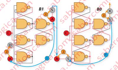
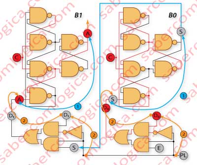
In Figure 1 we’ve represented a Right Shift Register with 2 bits width. B1 is the ETL for the bit of order 1, and B0 is the ETL for the bit of order 0.
- The bit D is prepared to go into B1.
- Output of B1 is connected to the input of B0 (B1→B0).
- Output of B0 is the bit X, going out of the circuit.
- Both A and S are at the inputs B1 and B0.
When the clock rises:
- Both A and S are memorized at B1 and B0, which is represented here by the cyan lines with the number 1.
- A is now at the input of B0, through the B1→B0 connection and D is now at the input of B1, which is represented here by the orange lines with the number 2.
- The bits at B1 B0 changed from SX, to A S.
- At the next clock (not shown):
- Both D and A are memorized in B1, B0 – cyan lines.
- B goes out through the orange arrow.
- The bits at B1B0 change from A,S to D,A.
The global evolution in B1B0 was (left→right):
DA→SX D→AS→X DA→SX
Left Bit Shifting
In Figure 2 we represented a Left Shift Register with 2 bits width. B1 and B2 are the same as before.
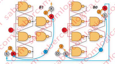
- D, the new bit, is at the input of B0.
- X, the leaving bit, is at the outup of B1.
- The output of B0 is connected to the input of B1 (B0→B1).
This is what is different about this circuit, when compared to the previous one. The remainder of its functionality is the same the above description, only in reverse. However, it would be an interesting learning exercise if you were to try and deduce the steps by yourself.
The global evolution in B1B0 was (right→left):
XA←SD X←AS←D XA←SD
In the global evolution showed for both the circuits, the shaded letters mean:
- Rose – Bits coming in.
- Blue – Bits that are leaving.
- Yellow – Bits being memorized.
Shift Verification
In Figure 3, we analyzed the behavior of two Shift Registers with 4 bit width, with a simplified representation, over several Clocks.
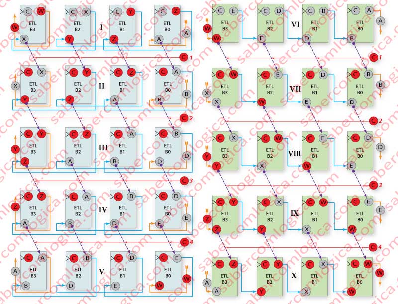
Notice that the bits released by the Left Shift in Frames I to V are those that are received by the Right Shift in Frames VI to X and vice versa. This way, we form a closed circuit, ex. two left and right shifts following each other.
- The blue arrows represent The ETL connections, and their direction.
- The orange arrows represent the circuit inputs and outputs, and their direction.
- The dashed violet arrows represent the memorization of the values in each ETL (input→output), under the effect of the Clock Rising Edge.
Left Shift
Frame I – Represents the initial situation of the Left Shift Register, with the Clock at low. W,X,Y,Z in B3,B2,B1,B0 are the bits to be shifted.
- The bit A is at the input of B0, and is the one being admitted.
- The connections of the ETL are B0→B1,B1→B2,B2→B3.
- B3 releases the bit W.
Frame II – 1st Clock.
- W is released by B3 and is going to Frame VII.
- A is admitted by B0, coming from Frame VII.
- The bits in B3,B2,B1,B0 are now X,Y,Z,A.
Frame III – 2nd Clock.
- X is released by B3 and is going to Frame VIII.
- B is admitted by B0, coming from Frame VIII.
- The bits in B3,B2,B1,B0 are now Y,Z,A,B.
Frame IV – 3rd Clock.
- Y is released by B3 and is going to Frame IX.
- D is admitted by B0, coming from Frame IX.
- The bits in B3,B2,B1,B0 are now Z,A,B,D.
Frame V – 4th Clock.
- Z is released by B3 and is going to Frame X.
- E is admitted by B0, coming from Frame X.
- The bits in B3,B2,B1,B0 are now A,B,D,E.
Right Shift
Frame VI – Represents the initial situation of the Right Shift Register, with the Clock at low. E,D,B,A in B3,B2,B1,B0 are the bits to be shifted.
- The bit W is at the input of B3, and is the one being admitted.
- The connections of the ETL are B3→B2,B2→B1,B1→B0
- B0 releases the bit A.
Frame VII – 1st Clock.
- A is released by B0 and is going to Frame II.
- W is admitted by B3, coming from Frame II.
- The bits in B3,B2,B1,B0 are now W,E,D,B.
Frame VIII – 2nd Clock.
- B is released by B0 and is going to Frame III.
- X is admitted by B3, coming from Frame III.
- The bits in B3,B2,B1,B0 are now X,W,E,D.
Frame IX – 3rd Clock.
- D is released by B0 and is going to Frame IV.
- Y is admitted by B3, coming from Frame IV.
- The bits in B3,B2,B1,B0 are now Y,X,W,E.
Frame X – 4th Clock.
- E is released by B0 and is going to Frame V.
- Z is admitted by B3, coming from Frame V.
- The bits in B3,B2,B1,B0 are now Z,Y,X,W.
Did you notice anything curious with the final results?
In Frame X is ZYXW, which is WXYZ inverted, this last being the starting point of Frame I.
In Frame V is ABDE, which is EDBA inverted, this last being the starting point of Frame II.
Conclusion: Two left and right shifts in sequence will reverse the bits of a number. In this particular case, B3→B0, B2→B1, B1→B2, B0→B3.
Parallel Load (PL) Shifting Registers
When we said that these circuits are commonly used for converting parallel to serial transmissions, we stated at a particular moment that “we place another set of 8 bits at the Register and start from the beginning”.
Who places them there and how is it done? Surely it’s not us who puts them there one by one?
Operations like these using these circuits emphasize the need to provide, at any given moment, the the ability to load the Shift Register with a new number to be shifted.
So what we want is a circuit that can perform two types of operations: Shift and Load.
And that’s the reason why we have the Parallel Load (PL) Shift Registers.
Before the input of each of the Registry Shift ETLs, we’ll have a doorman who, before each operation begins, asks you what you want to do. Then, the intended operation is executed, or rather, he performs an operation conditioned by the answer you gave him, a conditional operation.
So, what does he ask you?
Do you want to keep shifting? And we answer: “Yes, we do, (true, so we give him a 1)” or “No, we don’t (false, so we give him a 0)”. And here we have it, a human response, converted into binary, allowing one to choose between two possibilities.
Someone who does something like this is the Multiplexer, our old friend from long ago. And it’s precisely a MUX that will be before each ETL input, in place of the doorman.
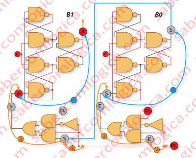
Since he has to choose between Shift and Load, we’ll set at its inputs:
- The output bit of the ETL connected with this one, for the situations where we want to Shift.
- The loading bit of a number with the same order as this ETL, for the situations where we want to Load.
In order for it to make a decision, we answer him with a bit called PL (Parallel Load). It Shifts with PL=1 (“Yes, it’s true, keep shifting”), and it Loads with PL=0 (“No, it’s false, don’t keep shifting”). This is the selection bit of these 2-to-1 MUX.
From here on, we’ll call these Registers, PL Shift Registers, PL meaning Parallel Load.
In Figure 4, we display a left PL Shift Register with Shifting as the chosen option. In Figure 5, a left PL Shift Register with Loading as the chosen option, both with a 2 bits width.
In these representations, as well as with the previous definition given to PL we define it as active at 0, meaning that the MUX executes a Parallel Load when PL is 0.
But it doesn’t have to be mandatorily so. It depends greatly on how the connections are made inside the MUX. This is what will define the active state of PL, in each case.
In Figure 5, since PL is 0, the parallel load D0 and D1 is selected.
The cyan lines show the path of the memorization (input→output) in B1 e B0.
The orange lines show the inputs D0 and D1, selected by PL in the MUX, which are now at the input of each ETL, prepared to be memorized in the next Clock.
In Figure 4, since PL is 1, the shifting of the bits is selected.
The cyan lines show the path of the memorization (input→output) in B1 and B0.
The orange lines show the inputs S and E, selected by PL in the MUX, which are now at the input of each ETL prepared to be memorized in the next Clock.
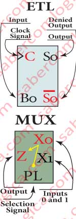
Figure 6 is a caption of the ETL and MUX, a reduced graphical representation of the one used in Figure 7. The yellow lines represent the input X0 or X1 being selected by PL in the MUX and set on the output Z.
In Figure 7, we display a left PL Shift Register, executing a Parallel Load, a left shift, and again a Parallel Load. Our goal is to help visualize how the events that activate the different possibilities are linked, and evolve within the MUX and ETL.
At the MUX input 1 are the bits to be shifted (selected by PL=1).
At the MUX input 0 are the bits to be loaded (selected by PL=0).
Frame I – Starting situation with the Clock at the down state. The number W,X,Y,Z is at the MUX input 0, prepared to be loaded into the Register by the PL. As PL is 0 this is the selected input, and these will be those whose value will be set at the inputs B3,B2,B1 and B0.
Frame II – 1st Clock. The bits W,X,Y,Z at the inputs of the ETL are memorized. The Parallel Load is complete. At the outputs of B3,B2,B1 and B0, we have now W,X,Y,Z.
The bits X,Y,Z are now at B3,B2,B1 MUX’s input 1. The bit A, the new one, is at B0 MUX’s input 1.
Although the new number to be loaded, R,S,T,U, is already at MUX’s input 0, since PL is 1, the MUX’s input 1, X,Y,Z,A, is selected to be shifted, and will be set at B3,B2,B1,B0’s inputs.
Frame III – 2nd Clock. The bits X,Y,Z,A at the ETL’s inputs are memorized. The left shift of W,X,Y,Z is executed, being now memorized in B3,B2,B1,B0 the bits X,Y,Z,A.
The bits Y,Z,A are now at B3,B2,B1 MUX’s input 1. The bit B, the new one, is at B0 MUX’s input 1.
The new number R,S,T,U to be loaded is still at MUX’s input 0, which will happen at the next Clock, since PL will be 0, and select the MUX’s input 0. The bits R,S,T,U are set at B3,B2,B1,B0’s inputs.
Frame IV –3rd Clock. The bits R,S,T,U at the ETL’s inputs are memorized, and the bits R,S,T,U are now at B3,B2,B1,B0’s outputs.
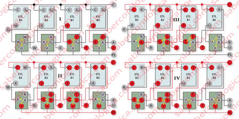
The bits S,T,U are now at B3,B2,B1 MUX’s input 1. The bit A, the new one, is at B0 MUX’s input 1.
The bits S,T,U,A will be at B3,B2,B1,B0’s inputs, since PL will be 0, and select the MUX’s input 1. Next Clock, they will be memorized at B3,B2,B1,B0.
We will leave it here for now.
Returning to our conversion circuit of a parallel to serial transmission, we mentioned that “The number to be shifted is loaded, then it is shifted bit by bit to the serial line, and when it’s done shifting, a new number is loaded”.
And how does it know when it’s done shifting?
Through a binary Counter circuit, which counts the bits being shifted, and sends out a warning when it is over, giving the signal to load the new number. This is what we will talk about next.
