
What is the Cache Memory
Now George is responsible for the archive of a great enterprise.
Each time someone needed a document asked it to George and he went into the archive aisle after aisle, he entered into the proper room, he looked for the proper bookshelf, he checked for the proper shelf, he fetched for a ladder in order to get access to the shelf, he sought for the proper folder and finally he took from that folder the requested document, he took a photocopy of it and put it back to place.
Then he ran all the way back handed the photocopy to whom requested it and, as he had more people waiting, he repeated identical paths to satisfy the next requests.
Thus George came to the end of each working day extremely tired from running during all the day the same paths. For that reason George thought of a way to not get so tired at the end of the day. It started by taking note of the places where he went to get the documents and verified that he was frequently going to the same places to get documents that were in proximity of each other or even the same documents several times.
So, he decided to take two photocopies of the requested document and also one photocopy of the documents that were close to it (in its proximity). And he kept all these photocopies in a large drawer of his desk.
Having done so, George noticed that now he had to move lot less times from his desk, since he often had already a photocopy of the asked documents in his desk drawer, only having to take a photocopy of this one in a photocopier that was near him. He also noticed that the more documents he had in his desk drawer, the less he had to go into the archive.
In the meanwhile, as the documents in his desk drawer were already a lot, he organized them within tabs identified by their address on the archive, i.e. the room, the bookshelf, the shelf and the folder.
From there on, when George was asked for some document he checked its address in the archive and searched the drawer tab for that same address. Then he checked if the asked document was there. If it wasn’t, George went into the archive to search for it, he took the two photocopies from it and one from the documents in proximity, and he brought them with him and kept them in the desk drawer, creating the tab for them if it didn’t already exist.
The result was positive, as they were increasingly less the times that George had to go into the archive. But a new problem arose. The desk drawer was completely full. But the method was working. His legs and back were a lot less painful at the end of the day where he got a lot less tired. It was not the time to stop.
So being, George imagined an improvement to its solution. He enlisted the help of a few colleagues, fetched for a bookshelf that was unused and placed it behind his desk. Now, he took always another photocopy of any asked document to put on the shelf. So when it needed to take documents from his desk drawer due to the lack of space he always kept them close to him, stored on the bookshelf.
And how did George know what documents to remove from the desk drawer when he needed room for new ones? Having this doubt, George started registering in the kept documents the number of times they were ordered. This way George could always know the least requested one within each tab and took the option to remove these.
As the bookshelf was getting filled, the less were the times George had to go into the archive. George was proud of its strategy and bragged from it to his friends. When the bookshelf got filled the times that George had to go into the archive were very few during the all working day.
And this is the Cache story, told in George’s person.
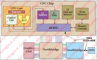
The Cache is the space where George kept his copies. The drawer was the L1 Cache (Level 1) and the bookshelf was the L2 Cache (Level 2). The persons who asked for the documents represent the CPU and George is the MMU (Memory Management Unit).
Therefore, the Cache Memory is one more strategy created by the human imagination to establish the best technical/economic commitment to get the best possible performance from the Main Memory and from the CPU.
When we say that all the working elements of the CPU (running program instructions and data) must be in the main memory for the CPU to use them, we complement this statement replacing the Main Memory by the Cache. This only complements the previously stated, since all the records in the Cache are duplicated from records that are in the Main Memory. Because the fetch in the main memory can become very slow, as we could observe in the previous chapter, we found a workaround where, playing with the principles of locality and temporality data blocks are collected from the Main Memory and placed in the Cache, trying to reduce the number of accesses required to the Main Memory during a program execution. And the results already exceed 95% access reductions.
The principles in which George was selecting the registration for the drawers were:
- The principle of spatial location, according to which there is a high probability that the registries on the proximity of an access are likely to be accessed on the following accesses and
- The principle of temporal location, according to which the registries with high probability of being accessed again are those that were accessed recently
Let’s focus on our analysis of the Cache and let George settle down.
The CPU fetches the data from Main Memory in Cache L1, which finds itself divided on two identical blocks although separated, the Cache L1 I (instructions) and the Cache L1 D (data).
This is the memory that the CPU knows. If the value is not found in the Cache L1, we have what is called a Cache miss. From here after it’s the MMU that manages the fetch to other levels in Cache or to the MM (Main memory), this one using the MC (memory controller).
Following George’s deductions we should have in these cache elements that are in proximity in the MM. This is the principle of Spatial Location.
For this to happen, having in mind the purpose to get the best access times to the MM, we must bring the highest amount possible of records, taking profit of the burst readings and thus reducing the average access time.
If we bring 64 bits in each reading on a burst of 8, we end up bringing 64 Bytes to the cache that are found on the proximity. This value can then become the Cache Block that corresponds to a Cache line. The movements to and from the Cache are always done in Blocks, so in our case, we are referring quantities of 64 Bytes.
The Compilers place the programs instructions in sequence in a specific place in memory and not evenly spread. Repeated instructions are frequent, as it is in case of access to certain sub-routines or the execution of loops. The data of constants and variables that is used by a program is also placed in proximity. So being, the bigger the cache and the blocks with data in proximity, the higher the chance of obtaining a good success rate. Statistically speaking, the chances of success are around 95% on the accesses made by the CPU to the Cache.
Cache Hit or Cache Miss are the names used to designate a successful fetch or a failed fetch in the cache and define the success rates on the accesses to the Cache.
Let’s now drop into our little memory and analyze the Cache with a new and simple perspective. Using the Byte as our word size. It’s important to remember that the memory addresses always refer to a Byte.
The Cache Cells
We are now going to assemble the circuits that allow the Cache memory to fulfill the purpose for which it was designed and its way of working.
The circuitry is simply the result of logic deductions that allow us to obtain the intended results. Any comparison with commercial circuitry is purely coincidental. We had not access to any of those circuits.
Certainly those circuits are more efficient than the ones we imagined since they are the product of thousands of hours of specialists work trying over and over again to improve the solutions.
Unfortunately, those circuits are not the best way to understand how we can achieve our objectives using logic gates, thus with 0s and 1s, in a simple way.
Thenceforth, the complexity will result on the sum of a lot of simplicities.
The Cache is made with static memory or SRAM (Static Random Access Memory).
Why static?
Well because the values in it stored are static (fixed) until they are changed or the power goes off, unlike MM, which is dynamic since the values it keeps in its cells need constant refreshment.
SRAM memorizes the values through transistors inserted on the sequential circuitry we already analyzed:
- The Flip Flop SR (Set Reset), which assumes different values on the output as the input variables assume state 1, making SET and RESET.
- The Flip Flop D is an improvement to SR with the advantage of being controlled by us, keeping the value of a data D according to the action of the clock signal or whatever other signal we want to use as a controller.
Based on these elements, we will now analyze how a static memory (SRAM) cell can be. In order to do it we’ll use the graphics in Figure 1 and Figure 2.
In the graphics, the signals RD and WR refer to the reading and writing and are active down, the signal CS (Chip Select) is active down, and the signal SB (Select Byte) represents the selection of columns that compose the byte we need to access.
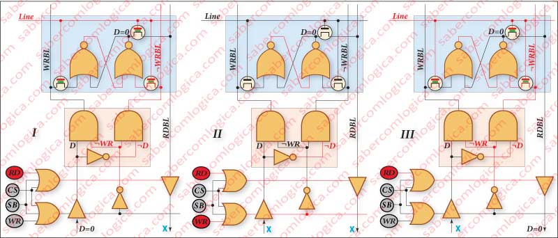
Let’s start by Frame I.
The cell is represented with a blue background. It is composed by a Flip Flop SR built with NOR gates, because we do not want it to be sensible to the situation where both input signals are down or 0.
The Flip Flop SR inputs are conditioned by two interrupters nMOS, which gates are connected to the line. Therefore, these only let information through when the cell belongs to an active line (the line is active high or 1).
And which information goes through?
At the bottom of the column we have two AND gates that connect the given D and its negation ¬D. At the other two inputs of the AND gate the ¬WR (the negation of WR) will turn on, that is, when WR is active (WR is active low or 0), its negation will work as the clock signal of a Flip Flop D composed by this set with the pink background, and by the Flip Flop SR of the active cell. The lines that come out of the pink set as inputs of the active cell are WRBL (WRite Bit Line) and ¬WRBL.
This way, we write in the Flip Flop SR the value that we want when the signal WR (write) is active.
In Frame II we can see the situation in which the cell stays inactive since the active line doesn’t connect to it. As we can see, making a logic analysis, the fact that both inputs are down does not affect the value of the output. The value kept in storage by the cell is maintained until change, even for reading or after reading, as we will see.
In Frame III the line of the cell becomes active again, but this time for a reading operation. The nMOS transistors are opened but there is nothing to write since the information has been cut by the BT (Buffer Tristate) that controls the writing in the cell. Yet again, we can verify that the value kept doesn’t change. The value can only be changed by a SET or a RESET which only happen when a value 1 is in one of the Flip Flop SR inputs. The reading is done using another line, the RDBL (ReaD Bit Line) that is connected to the Flip Flop SR output using one of the nMOS transistors whose gate is activated by the line.
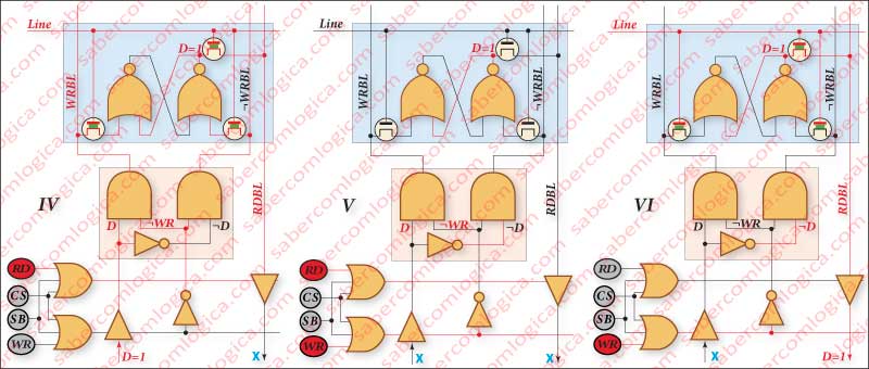
In Frame IV we write in the cell the value 1, following the same reasoning we did for the value 0. Yet again, we have a Flip Flop D in which the D is the value to write and the clock is done by the WR signal.
In Frame V we verify that the value 1 holds in memory, even when the line in which it is no longer is active.
In Frame VI we verify the reading of this value 1 and the fact that it has not been changed during all this process.
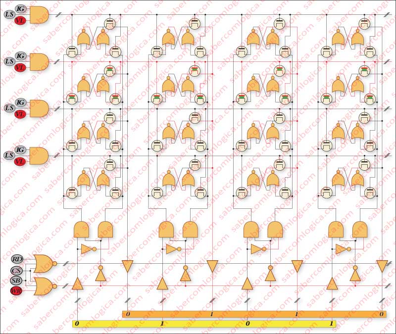
In Figure 3 we present what we consider to be an example situation of an access to a cache memory with 4 rows and 4 columns with the Tristate gates and all the other logic we referred, now dedicated to the several cells. The signals IG, LS and VL that select the active line are to be analyzed next in Cache mapping.