
The Division
To design the logic circuit that performs the division between two operands, we will have to interconnect most complex circuits, like those we’ve seen in the last Chapter.
We will decompose our reasoning in three parts:
- A first one, where we’ll look at the division of two unsigned binary, made by hand, determine its algorithm and insert it in the context of our circuit’s components.
- A second one, where we’ll develop the circuit’s diagram for a division in 2’s complement.
- A third one, where we’ll develop multiple frames representing the main circuit components to analyze the values evolution through them along the several iterations.
The Operation Sign
What we actually divide are the numbers modules, i.e., always positive numbers.
The division sign is mentally treated apart. If divisor and dividend’s signs are equal the quotient will be positive , if they are different, the quotient will be negative. The remainder will have the same sign as the dividend.
Thus, in the 2’s complement numbers division circuit, we’ll treat separately the sign through the most significant bit (the signal) and do the operation with the positive value of each number. When we divide (+20) by (-4) what we really do is divide 20 by 4 and apply the (-) sign to the result.
Hand Made Division Algorithm
Look at Figure 1 and tell us what it looks like. Yes, it’s just that, the Chalkboard of our old school where our master has written the division algorithm, to teach us how to make a division step by step.
And that’s just the same thing that we are going to do right now. But with binary numbers and taking the necessary conclusions in order to teach the computer how to do it. Like the computer we are going to do it step by step, digit by digit, never using our mental abilities to go quicker and do several steps into one.
The color lines try to show the path of the reasoning and are explained in the Figure caption. We will follow them to find the solution for the circuit. The small frames at left represent the subtraction we do each time we drop down one digit, to see if the divisor fits and if it does, to find the result. Here we convert the subtraction into an addition with the symmetrical trying to mimic the computer’s behavior. It’s the carry out of this addition result which will determine to the computer if it fits (1) or if it doesn’t fit (0). We’ll see further on why we can do this statement, but for now we will proceed to the algorithm. At left of each small frame there is a number which represents the iteration we are in. The two green and orange frames at the picture symbolize the decision making process regarding the carry out value coming from the small frames.
Well, it’s time to establish the binary division algorithm, describing the steps for its implementation and leaving it prepared for the computer. You can follow this steps with Figure 1 by clicking our touching it and placing it in a separate window. So:
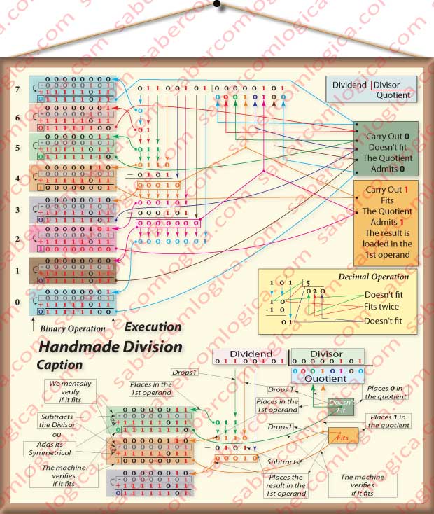
- Both operands are made into positive numbers.
- The operation result signal is calculated through the signs of the operands, knowing that + by + and – by – give +, – by + and + by – give –.
- The dividend’s first left digit is dropped down.
- In the small left frame it will be the 1st operand of the subtraction and it’s extended to 8 digits.
- Jump to step 8.
- Drop down the dividend first right next digit after the last dropped one.
- In the small left frame the 1st operand 8 digits are shifted left and the dropped digit is added at right.
- The divisor is subtracted from the 1st operand.
- If the result carry out is 0 it’s because the divisor doesn’t fit in the 1st operand, i.e. its bigger than it. Jump to step 11.
- If the result’s carry out is 1 it’s because the divisor fits in it, i.e. its smaller than it. The subtraction result extended to 8 bits takes the place of the 1st operand in the next iteration small frame.
- The value of the carry out is placed in the quotient at the right of the last digit, i.e. 0 if the divisor doesn’t fit in the 1st operand or 1 if it fits.
- If there’s no more digits of the dividend to drop down jump to step 14.
- Jump to step 6.
- The remainder takes the sign of the dividend.
- The result takes the sign calculated at step 2.
- The operation is finished.
The cooking recipe for an hand made positive binary number division is done. It’s now time to find the appropriate circuits to implement each of the steps of the algorithm. But before we must see how the carry out value affects the decision.
The Carry Out of a Subtraction between Positive Numbers
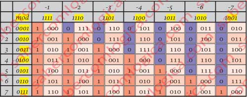
When we analyzed the Excess, we concluded that “When a subtraction operands have equal signs there’s no room to Excess“, even if the value of carry out is 1, what we saw it’s possible to happen.
For now, what we want to analyze is when the carry out assumes the values 0 or 1 and what that means.
A subtraction between two numbers actually is an addition between the first of them and the 2’s complement of the second. It was this way that we represented it in the small frames and it will be this way that the computer circuits are going to deal with it.
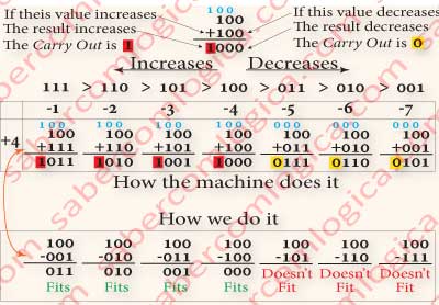
Let’s use the table in Figure 2 to follow this analysis. There we show, in each intersection of line number [from 001(1) to 111(7)] with column number [module of their symmetrical 111(-1) to 001(-7)] the result of their addition. We can clearly see a line which divides two different carry out behaviors. That’s the line representing each number addition with its symmetrical.
Remember that both operands are positive before being subtracted, the 2nd operand being then replaced by its symmetrical for the addition. Now take these final binary numbers, forget their signal and make their addition, just as we can see in Figure 3. As we can see the addition of one number with another equal or bigger then itself is not representable in the same order of bits (carry out 1) and that the sum of a number with another smaller than itself is representable in the same order of bits (carry out 0).
Once the positive numbers binary representation’s unsigned part grows from Zero as 100(4) >011(3) >010(2)> 001(1) and the negative one decreases from Zero as 100(-4)<101(-3)<110(-2)<111(-1) we can conclude that, being A the positive number and B the negative one:
- When the decimal value of A is ≥ than the module of B, then the binary representation of A unsigned part is ≤ than the one of B, thus their sum being not representable in the same order of bits (Co=1).
- When the decimal value of A is < than the module of B then the binary representation of A unsigned part is > than the one of B thus their sum being representable in the same order of bits (Co=0).
So, speaking in decimals and modules, if A≥B (B fits in A) the carry out is 1 and if A<B (B doesn’t fit in A) the carry out is 0. We can verify the correspondence: carry out 1→”fits” and carry out 0→”doesn’t fit”.
Logical Circuit Components
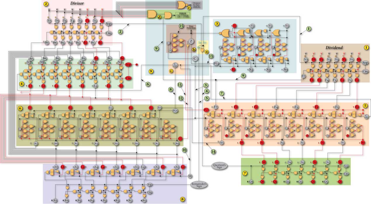
In Figure 4 is represented the division’s circuit for 8 bits numbers in 2’s complement. This circuit was built by putting together the several logical circuits we will find necessary to accomplish the several steps of the operation. It’s an imaginary circuit where any comparison with reality is pure coincidence. It was built together with its description. Our purpose was, once again, the logical reasoning and the logical deduction, this time clocked (logic).
In order to get there we are going to find the components to execute the steps of the algorithm between the circuits we already know, assigning one type of circuit to each of them. We can follow the description with Figura 4 and Figura 1 , clicking or touching the images to open them in a different window.
In Step 1 it’s said: “remove the sign and convert both operands into positive numbers”.
Each one of the operands will have to go through a Converting Circuit. The dividend through Circuit 1 and the divisor through Circuit 2.
What any of these circuits does is, by the action of the Sop and Cin signals of each respective operand, convert it to positive if it’s negative. It’s more or less like the part of the adder/subtractor circuit where Sop denies bits and Cin adds 1 when the operand is negative.
In Step 2 it’s said: “determine the sign of the result through the signs of the operands”.
For the interpretation of the circuit several signals who imply decisions and for determining their analysis outcome we created a Control Unit where all the small control circuits executing these tasks fall. We will call it Circuit 9. Inside this Control Unit each small circuit will be identified with a letter. Within this Step we’ll use Circuit 9a, a XOR gate where both operands’s signs are connected. If they’re equal (+ by + or – by –) XOR returns 0 (gives +), if they’re different ( – by + e + by – ) XOR returns 1 (gives –).
In Steps 3 and 6 it’s said: “drop down a digit from the dividend”.
For this step we’ll use a left Shift Register with PL which will load the dividend value at booting. For each iteration this Register releases one bit at left, the dropped down digit. We will call it Register 5.
In Steps 4, 7 and 10 it’s said: “In the left box we put the 1st dropped down bit extended to 8 bits (step 1), or we shift the digits to the left and add to the right the dropped down bit (step 2) or the subtraction’s result extended to 8 bits takes the 1st operand’s place running for the next iteration in the left box (step 10)”.
For all these steps we’ll use another left Shift Register with PL zeroed on booting, thus the 1st dropped down bit being naturally extended to 8 bits after its admission into the Register.
The parallel load happens when the divisor fits the 1st operand and the subtraction result is loaded into this Register. We will call it Register 6. This Register will always contain the 1st operand of the small frames addition. The digits getting into the 1st operand, thus the bits being admitted into Register 6, are the same digits being dropped from the dividend, thus the bits being released by Register 5.
In Step 8 it’s said: “subtract the divisor from the 1st operand”.
To execute this step we’ll use an adder/subtractor circuit which will simulate the behavior of the left boxes in the algorithm. We will call it Adder 4. This adder 2nd operand comes from Circuit 2, the divisor. It’s here that the symmetrical of the already positive and unsigned 2nd operand will be determined according to what we saw in the paragraph before (The Carry Out of a Positive Numbers Subtraction).
That’s why at this circuit Sop and Cin will always have the value 1, not depending on any operand signal. Actually the value getting here through the action of Circuit 2 is always positive, having to be converted into their symmetrical in order to be included in this addition operation. The 1st operand is always contained by Register 6, the reason why it will get to here through a connection between them. This circuit returns, beyond the operation result, the final carry out value which will be used by the Steps 9, 10 and 11 of the algorithm.
In Step 11 it’s said: “the carry out value is placed on the first digit to the right of the last one in the quotient”.
Here comes another left shift register to admit them at right and shift them left. Maybe not! We already have a Register that releases one bit at left for each iteration and we can use it to take a bit at the right for each iteration. The Register 5 is good for both functions, specifically for this one. As it will simulate the drop down of dividend values it will simulate the charge of values in the quotient.
In Steps 9 and 10 it’s said: “the addition Carry Out value is evaluated and decisions are made on its basis. In both steps its value is placed in the quotient. When its value is 1 then the addition’ result is loaded into the 1st operand.”.
One more task for the control unit, this time through Circuit 9c, which forwards the carry out value into the Register 5 as a quotient digit, when it left shifts the digits releasing the dropped down bit from the dividend. It forwards the carry out to Register 6 too, where through PL it will cause to load the addition result if its value will be 1.
In Step 12 it’s said: “if there isn’t more digits to drop down from the dividend then jump to step 14”, or in other words, “if there isn’t more iterations to do then jump to step 14”.
In order to state this we will use a Descending Counter with PL and Zero Detection which we’ll call Counter 3, active at 1. It loads (PL) the number of digits of the dividend (the number of iterations), it runs the countdown for each digit dropped down and for each Clock and when it reaches zero (Z) it does what is written in the algorithm step 14.
In Step 14 it’s said: “the dividend sign is set to the remainder”.
As the operands were converted into positive to determine the value of the division, now we have to convert the results according to the sign they’re given. In this case, for the division remainder, it’s the dividend sign. To do this we use an Converter Circuit which we will call Circuit 8. To know what’s the value that should be at this circuit’s inputs to be converted, let’s look at the last frame on the algorithm left side. We can see that the remainder will be the 1st operand, the one in Register 6.
Yeah, but it seems like it might not always be the case!
It will like that if in the last iteration the divisor doesn’t fit in the 1st operand, i.e. if the operation Carry Out is 0. But if it fits, thus the carry out being 1, then the addition is executed and the remainder will be its result, the output of Adder 4, who has not enough time (the poor one) to be memorized in Register 6 before the result is read.
In next paragraph we will see about signals propagation.
So, the remainder value can come from two different locations, depending on the value of the carry out. Hence the presence of a 2 to 1 MUX in this Circuit 8. Each of these two possible outcomes is connected to one of the MUX’s inputs and the selection bit is the carry out value forward herein by the Circuit 9c. The remainder sign value, forwarded herein by the Circuit 9a, is set directly to the remainder highest order bit (R7) and to of this circuit Sop and Cin values, this way determining if there’s room for the sign inversion.
In Step 15 it’s said: “the sign calculated at step 2 is set to the result”.
Here too we’ll have to convert the operation’s result sign according to the sign determined for it. In order to do it we’ll use another Converter Circuit which we will call by Circuit 7. In this case the sign will be the one calculated in the algorithm’s step 2, in this circuit given to us by the Circuit 9a. It’s value will be set directly to the result highest order bit (Q7) and to this circuit Sop and Cin values, this way determining if there’s room for the sign’s inversion. The result value is the quotient value, thus the one in Register 5.