The Division Logical Circuit

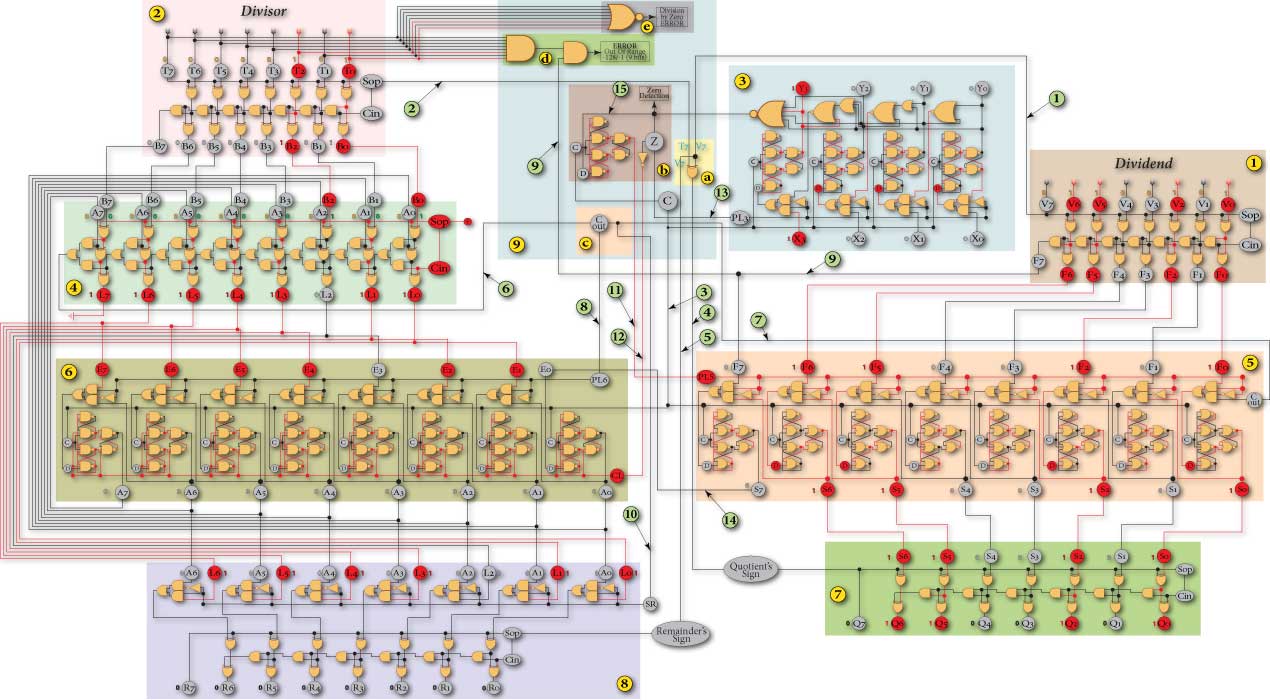
In Figure 1 is represented the division’s circuit for 8 bits numbers in 2’s complement. This circuit was built by putting together the several logical circuits we will find necessary to accomplish the several steps of the operation. It’s an imaginary circuit where any comparison with reality is pure coincidence. It was built together with its description. Our purpose was, once again, the logical reasoning and the logical deduction, this time clocked (logic).
In order to get there we already found the components to execute the steps of the algorithm, in the previous article. Now we are going to implement the circuit putting all the components together and interconnecting them. We’ll look essentially to the signals propagation into the circuit along the clock cycle and to the behavior of each component regarding that same clock.
Implementing the Circuit
By implementing the division algorithm into a circuit, all the components have to be interconnect with each other. In order to do this we’ll need the correct knowledge of each component behavior. We’ll give special attention to the signal propagation along the circuit and to the resulting component behavior regarding their interconnections. The analysis of the internal logic of each circuit, in issues that have no relation to the above set forth priority, is a matter that this time we leave to your analysis, what you can do using the circuit diagram. You can follow the description with Figure 1 from the previous article together with this Figure 1 once opened in different windows.

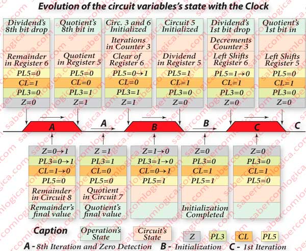
We recall the composition of the clock cycle, here shown in Figure 2.
The circuit we are implementing is shown ) with the clock low (C=0) and at the end of the circuit’s initialization cycle. We considered that all the modifications and propagations to happen during the cycle are completed. The variables state at the beginning of this cycle , dependent on what happened in the previous cycle (the detection of Zero), its variation during this cycle and its state at the end of this cycle, which will influence the next cycle, will also be considered.
Circuits 1 and 2
What these two circuits do, we have already seen in their assignment to the algorithm Step 1. Now we will look at their connections.
The Circuit 1, the dividend, is directly connected to the inputs for the Parallel Load of Register 5.
The Circuit 2, the divisor, is connected to the 2nd operand of the Adder 4, there remaining unchanged during all the operation.

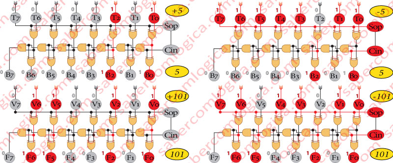
In Figure 3 we can verify that the actually realized division is of 101 by 5 whatever the sign of dividend and divisor is [(+101) or (-101) or (+5) or (-5)]. After passing through any of the circuits 1 or 2 their representation will always be the one of the unsigned integer of the number, 01100101(101) e 00000101(5).
Notice that circuits 1 and 2 have only 7 bits and the ones they connect to have 8 bits. Bearing in mind the fact that we are dealing with 8 bit 2’s complement numbers, now positive and unsigned, what’s the 8th bit good for? This issue has been addressed at the multiplication, in the Binary Arithmetic chapter. This time it’s yours the task to understand why.
Circuit 3
This is the Counter 3, assigned to the algorithm’s Step 12 where we already described what it does. PL3 is the Parallel Load signal for this circuit and its value at the end of the circuit initialization cycle is 0.
Shouldn’t PL3 have the state 1 at this point?
Apparently yes, as in this circuit PL is active at 1 and a Parallel Load has just been made, thus with PL3 at 1. Actually, during the clock immediately before this one, where the Zero detection happens, Z value becomes 1 and hence PL3. So being, PL3 is 1 and the value to be loaded is at this Circuit Edge Triggered Latches (ETL) inputs when the rising edge of the clock that we are analyzing happens. The Parallel Load is executed and that value memorized.
Now it’s time for the signal propagation. Once memorized this value and during this clock, Z becomes 0 and hence PL3. So, at the end of this cycle PL3 will be 0 with its task fulfilled and prepared to let the countdown begin at the next cycle.
Circuit 4
This circuit is the Adder 4, assigned to the Step 8 of the algorithm, where the essential we had to say about it was already described.
Circuit 5
This circuit is the Register 5 assigned to the algorithm Steps 3, 6 and 8, where it was already described in what it does, what it releases, what it loads with PL and the bit it admits.
We will analyze here how to solve problems resulting from signals propagation demanding a good knowledge of the clock cycle components and highlighting the importance of clocked logic in the synchronisation of scattered events in a circuit or even in the computer.
The Relay Racers
At the rising edge of this clock the values in Register 5 are left shifted. Our 1st relay racer is the released bit (the highest order one) which be the lowest order one of the bits’s set memorized by Register 6 as 1st operand for this iteration.
This is the 1st operand value to propagate in the circuit during this clock. Once arrived at the Adder 4, the divisor its subtracted to it producing a carry out whose value is assigned to our 2nd relay racer, which will run through Circuit 9c directly to Register 5.
Once arrived, our 2nd relay racer will stay at the order 0 ETL input, but a lot after the rising edge of this clock. It will stay there, waiting for a new cycle.
Wasn’t it this the bit that should be admitted as quotient into the Register 5 during this iteration, thus when it shifted left?
Indeed it was, and the problem is precisely there. Their fellows are gone and as it arrived late it was left back and they took another one with them, the one which was yet at the ETL’s waiting for our friend to replace it.
This way everything will be wrong, won’t it?
Yes it will. For each shift happening in a Register one bit has to be admitted and the others can’t stand waiting for it. Its fellows are sprinters and aren’t guilty of its preference for relay races. But they have to be forced to wait for it.
How can we solve this?
Notice that in this case the problem arises from the fact that the value of the bit being admitted into Register 5 during a shifting depends on the value of the bit leaving due to that same shifting.
So, if the shifting would happen only after it arrives, the problem would be solved?
Correct. And we could achieve it if Register 5 ETL would respond to the clock falling edge. This way, the value being admitted during its left shift would be correct, as our 2nd relay racer would already be at its place.
But, so being, the bit memorized in Register 6 won’t be correct because as Register 5 hasn’t yet been shifted that bit hasn’t yet been released?
Well, thinking a little deeper in the question we think that it won’t be quite like that. The bit being released is the highest order bit of Register 5 outputs and is connected to the lowest order bit of Register 6 inputs. Thus, due to this connection, the bit to be released is already at Register 6 input 0 and, at the clock rising edge it’s this value to be memorized, following the steps just described for it as 1st relay racer carrying the correct value, so ensuring that the 2nd relay racer will have the correct value too when arriving to Register 5 input 0, just before the left shift happens.
At the clock falling edge the Register 5 is left shifted, our 2nd relay racer gets into the quotient and the released bit disappears forever. It will be the following order bit, now the highest order one which will be released in the next cycle, that will be connected with Register 6 input 0 from now on.
It seems now it’s everything OK with this circuit.
Yes, but just apparently. Everything is OK for a normal iteration. But not for the circuit booting.
The Parallel Load

The clock cycle we should be analyzing is the one of Register 5 booting. At this cycle we don’t have an iteration but a Parallel Load, precisely of the next operation quantity of iterations. At this Register the Parallel Load signal is represented by PL5 and is active at 1. In the analysis we’ve just done to the Circuit 3, we verified that Z becomes 0 during this clock. As PL5 is connected to Z it becomes 0 too. So, when the clock falling edge happens PL5 will be 0 and the Parallel Load isn’t made. While this Register was sensitive to the clock rising edge this problem didn’t exist, as there PL5 was still 1.
So, how are going to solve this?
We are going to delay PL5 propagation regarding Z in one clock.
And how can we do that?
By interposing an Edge Triggered Latch (ETL) in the line that connects Z to PL5, thus having Z at its input and PL5 at its output. That way, during the clock where Z becomes 1 (the Zero detection one), its new value will stay at the ETL input. At the following clock rising edge, the one of the circuit’s booting which we are dealing with, PL5 becomes 1. During this clock, Z will become 0 as we’ve seen, but its new value will stay at the ETL input, thus PL5 remaining 1. At this clock falling edge the dividend will be loaded into Register 5 as previewed. In Figure 4 we illustrate the evolution of the variables values and of the circuit state from the clock rising edge of the Zero detection cycle until the clock falling edge of the 1st iteration cycle.
Circuit 6
This circuit is the Register 6 assigned to the algorithm Steps 4, 7 and 10, where it was already described in what it does, what it releases, what it loads with PL and the bit it admits. When the carry out of the Adder 4 is 0, the bits are shifted left and admits the bit released bt Register 5, the one dropped down from the dividend. When the carry out of the Adder 4 is 1, the bits from this adder outputs are loaded and left shifted, being admitted the bit released by Register 5, the one dropped down from the dividend.
And it does all this in one single clock ? Load and shift are made in 2 distinct cycles. We are putting them together in one only cycle? How is that?
Yes it’s true. And actually we don’t have all that time to do it as the other circuits won’t wait for this one. During the first of this 2 cycles the 1st operand has to be at the Adder 4 for the divisor to be subtracted from it. Well, then we’ll have to find a trick to make the two operations at once. Actually when Register 6 loads it doesn’t shift left.
And what about if we could load in a such way that a left shift is simulated?
Yes, it’s possible. If we connect the Adder 4 outputs to the upper order Register 6 inputs, i.e. L0 to E1, L1 to E2, and so on, leaving E0 connected to Register 5 highest order bit, the released one, the value to be loaded is already left shifted at Register 6 inputs. This way, when the parallel load is executed the loaded value will already be left shifted. Two in one. Great.
And what about the bit L7 from the Adder 4 outputs?
That would be the bit to be released during the Register 6 left shift. Not connecting it we simulate it’s release. Register 6 initialization is made executing a Clear to it at the clock rising edge of this cycle,the one after the Zero detection. As a relation exists between the Zero detection and the Clear action, we must connect Z to CL (Clear). The value of Z becomes 1 during the clock cycle where zero is detected. So, its value will be 1 at the clock rising edge of the initialization cycle, the same where the Clear will be executed. So, in Circuit 9b, the denied value of Z will be connected to CL, as it is active at 0.
Circuit 7
This circuit is the Circuit 7, assigned to the Step 15 of the algorithm, where the essential we had to say about it was already described.
Circuit 8
This circuit is the Circuit 8, assigned to the algorithm Step 8, where the essential we had to say about it was already described.
Circuit 9
This is the Frame 9, the circuit Control Unit. It contains several small circuits analyzing signals produced inside the circuit and transforming them to be used by other components. The Circuit 9a analyses the operands’s signs and determines the signs:
- of the remainder, sending it to Circuit 8 and
- of the result, sending it to Circuit 7.
The Circuit 9b analyses the Zero detection (Z), assigning Z value to PL5 and PL3 and Z’ denial to Circuit 6 CL and informs the outer circuit about its value at any moment. The Circuit 9c reads Circuit 4 carry out and assigns its value to PL5, to PL6 and to the selection bit of Circuit 8 MUX. The Circuit 9d verifies if the divisor value is (-1) and the dividend value is (-128) simultaneously, what would return a result of (+128). This result is possible between all the possible operations within the circuit and its binary result 1 0000 0000 wouldn’t be representable in 8 bits. If this is the case an error signal is sent to the outer circuit. The Circuit 9e, when the division of a number by zero is detected, sends an error signal to the outer circuit.
