
The multiplication
With the knowledge we acquired so far, we will certainly be able to mount the multiplier circuit for 4 bit numbers in two’s complement and understand how we get there.
We will do it with a circuit that fulfills the reasoning we use in multiplication made by hand, according to the algorithm that we will develop following with Figure 1. What we have learned so far only allows us this solution.
We’ll do it because it’s important to exercise the logical reasoning concepts so far acquired with a more elaborate operation and because we will do it with only 4 bits for a two’s complement representation.
Its Algorithm
We are going to deal the same way with numbers with equal or different sign. Just as we do with our decimal numbers. Actually, when we multiply two numbers, our operation doesn’t act over the sign, i.e. the sign is dealt separately. Plus by plus is plus, plus by minus is minus, minus by minus is plus. The numbers are multiplied in module and at the end of the operation we apply the sign to the result.
If we multiply (-5) by (+4), actually what we do is multiplying 5 by 4 and give the result the sign resulting from the signs operation, plus by minus equal minus, thus (-20).
Thus, our multiplying operation has to be divided in two phases:
- Determination of the final sign of the operation.
- Multiplication of the operands in module, i.e. by their absolute value.
The module of one number represents its absolute positive value. In Base 10 it’s enough to withdraw the signal from the number and we have its module. But in Base 2 it just won’t be so easy. If it’s a negative number then we have to find its symmetrical and ignore the zeros at left, as they are no longer a signal.
Now it’s time to see how we multiply two numbers in module. Let’s establish the multiplication’s algorithm following Figure 1.
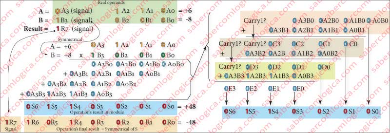
- We write the multiplicand (the one being multiplied).
- We write the multiplier (the one who multiplies) below the multiplicand and aligned digit by digit starting from the right.
- We draw a line below these two.
- We multiply all the multiplicand digits, one by one, by the first multiplier digit, writing the result below the line and under the multiplier digit, starting from there to the left with the next multiplicand digits. If its the case the final carry 1 goes to a next column.
- If the multiplier doesn’t have more digits we jump to step 11.
- We multiply all the multiplicand digits, one by one, by the multiplier digit immediately at left of the previous one. The first result is written under the existing line of previous multiplication and vertically aligned with the multiplier digit, starting from there to the left with the other multiplicand digits. If its the case, the final carry 1 goes to a next column.
- If the multiplier doesn’t have more digits to the left, we jump to step 9.
- Jump to step 6.
- Draw a line under all the lines of results obtained.
- We add the values of all the result lines column by column, writing them vertically aligned with the added column and under the drawn line.
- The obtained value is the result of the multiplication.
And now, how can we explain this to the computer in its language?
We will begin by applying this algorithm to the multiplication of the number A3A2A1A0 by the number B3B2B1B0. Let’s look at the first result of the operation, where it’s written A0B0, i.e. the result of the multiplication of the first multiplier digit by the first multiplicand digit, or the binary multiplication of the bit A0 by the bit B0. The binary multiplication is represented by the AND operator:
0.0=0, 0.1=0, 1.0=0 and 1.1=1
will be the possible results of the binary multiplication, which match the truth table of an AND gate whose inputs are A0 and B0. Thus, in order to get the result of the multiplication of each multiplicand bit by each multiplier bit, we must connect each pair to an AND gate in the combinations that concern us in each position.
The result of the multiplication is obtained by the sum of the columns resulting of the previous multiplication according to the algorithm. As the adder circuit only allows the addition of two bits we must execute this addition through the decomposition that is shown in Figure 1-21, adding two lines each time as follows:
- The two first lines.
- This result with the 3rd one.
- This result with the 4th one.
Each partial adding is shadowed with a different color Notice that A0B0 corresponds directly to the bit S0 from the operation’s result. Thus it won’t go into the adder circuit. The first bit of the result of each adder goes directly to the result, thus doesn’t go into the following adder. The carry out of each adder circuit will be added with the last bit of the following adder.
The Logical Circuit
Let’s support our analysis in Figure 2, mentioning from now on their frames where are localized the partial circuits being analyzed.
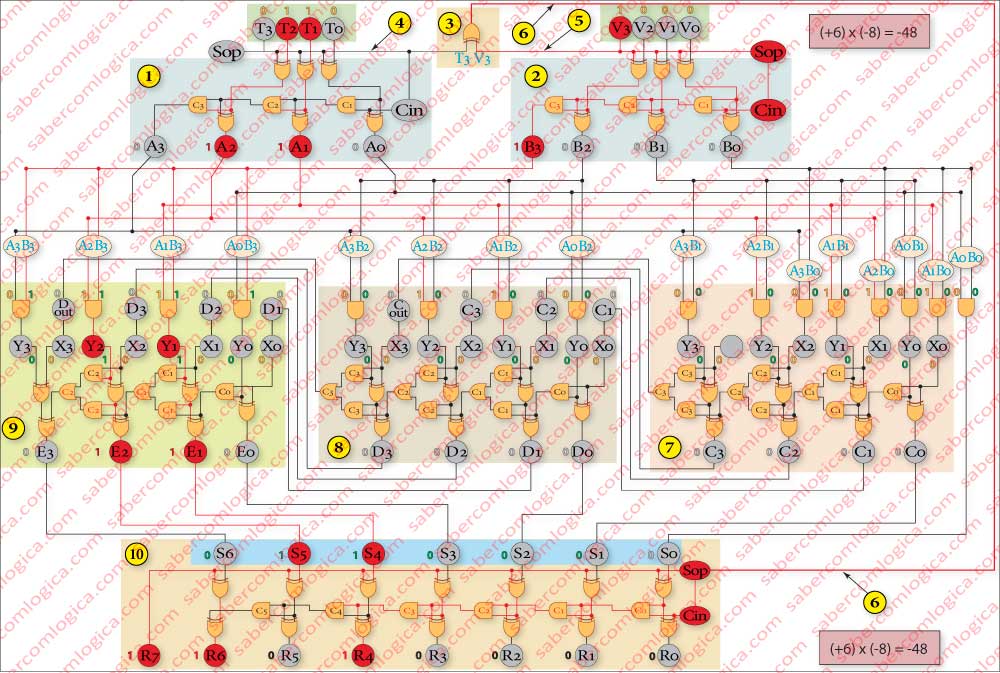
In what concerns the sign, the rule that determines whether the result sign is positive (0) or negative (1) as the operands signs are equal or different, corresponds once again to the response of a XOR gate whose inputs are the operand signs, as in frame 3. If they are equal the result will be positive (0) or XOR false. If they are different the result will be negative (1) or XOR true. We just have to connect to this XOR gate input the highest order bits of the operands and its output directly to bit R7 and to frame 10 as Sop and Cin.
Now,we will look to the operands. If anyone of them is negative we define its symmetrical and begin the operation with it. Loud and Clear. But in English.
How will the computer know if a number is negative and acts accordingly in all possible situations?
Let each operand’s sign’s representative bit speak, as we can see in frames 1 and 2.
- The circuits 1 and 2 convert one number into its symmetrical. The number in circuit 1 is positive. The number in circuit 2 is negative.
- Each operand bit is connected to a XOR gate together with Sop, being this the operand’s sign. The operand’s bits will be denied if the operand is negative.
- The outputs of these gates are the inputs of an adder circuit which will add Cin to the obtained number.
- The result from this adders will represent the operand or its symmetrical, as it is positive or negative.
- Lines 4 and 5 connect the operands signs T3 and V3 to the previously referred XOR gates, to Sop and Cin and to the XOR gate of frame 3.
Notice that the last carry out of these circuits is inserted in a new order 3 bit for each operand, A3 and B3.
But their order 4 bit has been withdrawn cause it was the sign. How is this?
This has to do with two’s complement representation. The smaller negative number representable with 4 bits (-8=1000) has a symmetrical that can only be represented in 5 bits (+8=01000) or 4 bits in module (8=1000). If we wouldn’t have the new order 3 bit we would have a wrong result in circuit of frame 2.
The multiplication of the so obtained operands bits, by AND gates which return its result, is introduced in the circuits of frames 7, 8 and 9, where lies each one of the partial additions represented in the algorithm. These circuits are simple adders where the order of the operands is reproduced as it is in the algorithm. The result which comes from these circuits, i.e. the result of the two operands multiplication in module, is represented by the bits S6 to S0.
Now the values of S6 to S0 are treated by the circuit in frame 10, identical to the circuits 1 e 2. In this circuit, the values of Sop, Cin and R7 are defined by the result sign, transported by line 6 until here.
From this circuit, where the symmetrical of the result S6 to S0 is calculated if it is negative, comes the final result, represented by the bits R7 to R0.
This will not certainly be the method that we’ll use to create a multiplier circuit. Just look at the picture of the algorithm that we followed or at the circuit that performs it, and you can realize that its size if we were working with 64 bits would not be feasible. The efficient solution for such cases is obtained by using circuits that are built based in more complex logical circuits that we will analyze further on. Those circuits will allow us to understand the CPU and to execute the Division and even the Multiplication but now through iterative methods.
But, before going to the analysis of these circuits we will make an interruption in order to unwind our minds. We will make a detour through the digital image and sound and try to show, always through the journeys of the bits, how the computer presents in an analogical fashion the images and the sounds he keeps in digital representation. And how it captures the analogical human world of images and sounds to convert it into a binary representation that it will keep in storage.