
The Transistor
From abstraction to reality
When we consider the materialization of logic gates, we have to descend from abstraction to concrete and understand how we can achieve such reasoning in terms of machine.
And the machine, as I said, is a set of circuits that we try to put playing the thought of Mr. George Boole.
Thus, concepts related to electricity will be from now on, part of our reasonings.
For now let’s talk a little about electricity, but obviously in a very basic, the necessary and sufficient one in order to pursue our goal. The Materialized Logic
Electricity
Electricity is a physical phenomenon. We can not see it or pick it up, but we can know when it is present.
To understand what electricity really is we will start by talking about atoms. The atoms are the building blocks of nature. Everything that exists is composed by atoms. Air, water and solids. Atoms have minute size. A grain of sand is made up of millions of atoms.
Compare the atom to our solar system. In the center there is the nucleus and around it revolve small particles. The center is the sun and the planets are the small particles.
The center of the atom is it’s core, composed of neutrons and protons. The electrons revolve around it.
Why do the electrons revolve around the core?
Because they are attracted to it. Protons have a positive charge and electrons have an equal negative charge. So, as in the solar system, the electrons are placed in long orbits around the core, so that the attraction between the two offsets the electron’s tendency to go out of orbit, a value dependent of its mass and velocity which we call the kinetic energy. When an atom is in equilibrium it has an equal number of protons and electrons.
In some metals, such as copper, electrons revolve in orbits so far away from the core that easily can release it. Electrons, by freeing up from their orbit and moving along the metal, generate what we call electricity, or electrical stream, which is nothing more than electrons in movement or a stream of electrons. And their movement propagates along all metal lines that are in connection.
The electrons flow in closed circuits. If we open the circuit, we interrupt the flow, because the electrons stop moving. Is by this manner that we turn on or off one lamp via a closed or opened switch, allowing or not the electrons to flow through the circuit which leads to the lamp filament, making it incandescent through the heat which its stream raises therein, producing light.
The filament lamp becomes incandescent because it offers resistance to the electrons flow. Resistance is the opposition to the flow of electrons that a particular material offers. To the value of this resistance is given the name of impedance.
A highly conductive material has a zero or nearly zero impedance value, i.e. it doesn’t offer any resistance to the flow of the electrons. An insulating one is a material of infinite resistance, i.e. it doesn’t allow the electrons to flow through it.
Once done this basic approach to electricity and understood the role of electrons in its movement, let’s proceed with our work.
We’ll start by talking about the thermionic valves or vacuum tubes, in order to better understand the approach to transistors.
Thermionic valves
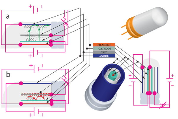
Let’s analyze specifically the operation of a triode. A valve is, as the name indicates literally, a controller of electric stream’s flow passing through it, as are faucets for water. The components of the valve, as we can see in Figure 1, are contained within an ampoule in which vacuum is created, in order to decrease the resistance to the flow of electric stream.
Their composing elements are as follow:
- A Filament, or electrical resistor, whose sole purpose is to produce heat;
- A metal plate connected to the negative pole which is called Cathode;
- Another metal plate connected to the positive feeder that is called Anode;
- A Grid (which can be designated as such because it is a metal mesh) connected to the negative pole of the power supply through a circuit in which is interposed a potentiometer.
The anode, which is connected to the positive pole, loads positively and drains the free electrons to the source. The cathode, which is connected to the negative pole, is saturated with electrons. This way, a potential difference between cathode and anode is established. The cathode, when heated by the filament, can liberate electrons which flow through the void (the ampoule is under vacuum) from the cathode to the anode, thereby establishing an electric stream that passes through the valve as shown in Figure 1-a.
Decreasing to zero the resistance of the potentiometer, a negative voltage is applied to the grid, thus saturating it with electrons. As charges with the same polarity repel themselves, the grid prevents the movement of electrons from the cathode to the anode through it, thus interrupting the flow of electrons through the valve, as seen in Figure 1-b.
In the intermediate positions of potentiometer’s regulation are obtained the intermediate levels of electric stream flow (or flow of electrons ).
For instance, this was the way how the volume control of an ancient radio set built with vacuum tubes was made.
But the vacuum tubes were extremely sensitive (as they were glass lamps), bulky, consuming huge amounts of energy and slow to warm up before they can start to work.
ENIAC (Electrical Numerical Integrator and Calculator) was the first large scale electronic digital computer. Created in February 1946, it weighed 30 tons, it was 5,50 m high and 25 m long and occupied an area of 180 m². It was built on steel structures with 2.75 m high and had 70,000 resistors, 17,468 vacuum tubes, 10,000 capacitors, 1,500 relays and 6,000 switches. According to Tom Forester, when triggered for the first time, the ENIAC consumed so much energy that lights flickered in Philadelphia. The ENIAC could do five hundred multiplications per second. It becomes clear that the vacuum tubes, although fulfilling their function, needed an urgent replacement. The same manner that in this work they where useful to introduce the topic, in reality they were useful to sharpen the wit of man in finding their replacement.
And this was the way how transistor arose.
Transistors
Transistors have an equivalent behavior to the one of the vacuum tubes. There are several types of transistors according to the kind of application for which they are intended.
To demonstrate how the abstract logic is physically materialized, we’ll use nMOS transistors from the MOSFET (Metal Oxide Semiconductor Field Effect Transistor) transistors family, although inserted in circuits with the architecture of DCTL (Direct Coupled Transistor Logic) transistors family in the construction of logic gates whose behavior we want to physically perform.
The reason to do so lies in the fact that DCTL architecture is the simplest to understand, therefore the one we believe to be the most suitable for the didactic propose of our work.
The DCTL family of transistors was never implemented in the construction of Integrated Circuits (IC).
Other families came and were used in IC , by the incorporation of resistors and the use of different architectures, of bigger difficulty to understand and thus not good for our propose.
In any case all of them are virtually extinct and replaced by transistors of the MOSFET family (Metal Oxide Semiconductor Field Effect Transistor), which integrate almost all of the current Integrated Circuits.

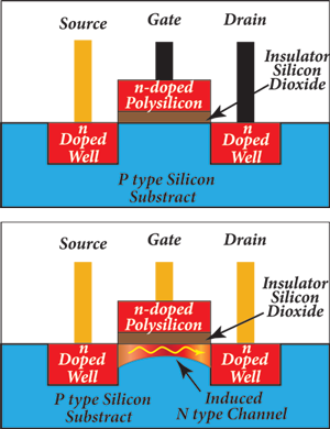
In order to better understand the following text we recommend you first read the next paragraph, which describes the manufacture of an integrated circuit with nMOS transistors. For that propose it’s important to know the composition of an nMOS transistor:
- The Source (N)
- The Drain (N)
- The Gate (N)
- The Base or Substrate (P)
as we can see in Figure 2 as a graphic scheme.
Among the many differences between the MOSFET transistors family and the previous transistors families, to whom was given the name of bipolar, we emphasize the fact that in the MOSFET family the Gate is insulated from the Source and Drain, reason why the power applied to the Gate does not flow to the Drain, thus reducing the power consumption and the quantity of components (e.g. resistors), increasing its integration capacity.
We’ve mentioned a lot of strange names like silicon, semiconductor, field effect, integrated circuits and so on. It’s now time to actualize our dictionary and try to understand what all this means.
The MOSFET transistors family includes:
- nMOS transistors, where Gate, Source and Drain are negatively doped and integrated in a positively doped substrate,
- pMOS transistors, where Gate, Source and Drain are positively doped and integrated in a negatively doped substrate and
- CMOS transistors, always composed of two transistors being one nMOS and one pMOS, thus giving rise to its name CMOS (Complementary Metal Oxid Semiconductor).
CMOS transistors are the most widely used, particularly in microprocessors and memories. However the architecture of its circuits is much more complex and therefore less easy to understand for the purpose of this part of our work, reason why we are going to focus into the nMOS transistors.
At the end of this chapter we will discuss the CMOS transistors, analyzing their manufacture and integration in the logic gates NOT, NAND and NOR.
The material currently used for the transistors manufacture is the silicon. Silicon is an electrical insulator due to the shape of its atoms electronic connections, generating a highly stable electronic network. The Silicon allows, through the introduction of impurities, to change in specific locations it’s stable structure, converting it into unstable structures of type P (Positive) or N (negative). It’s this Silicon property that turns possible the transistors construction into thin pure silicon crystal blocks called Wafers.
The transistors that concern logic, are created in purified silicon wafers as part of integrated circuits. At the location of each transistor, the wafer is submitted to a doping process (ionization), being introduced tightly controlled amounts of selected materials known as impurities.
These impurities, which are introduced between the silicon atom structure, steal or give electrons to the silicon atoms, generating respectively the P or N silicon substrate, as that substrate is positive (it has atoms with electron holes) or negative (it has atoms with electron overflow).
If the impurity has one electron in excess, an electron overflow is created in the crystal structure. If the impurity misses one electron, an electron gap is created in the crystal structure (it works like a mobile hole in the crystal structure).
The nMOS transistor works through the stream of electrons which it can generate between the two N wells, source and drain, incorporated in the P substrate, as we can see in Figure 3.
The Source is linked to the negative pole and the Drain is linked to the positive pole of the power supply. The Gate, which is linked to the positive pole, can cut or allow the flow of electrons through the Base. The Base (the part of the substrate under the Gate), works like a plug to the flow of electrons between the Source and the Drain.
When voltage is applied to the Gate (Figure 1 below) the positive state of the Gate and the generated Field Effect throws away from the Base the atoms with holes (positive atoms) of the P (positive) substrate and the electrons from the Source and from the Drain are attracted, filling the space left by the P atoms and thus creating the flow of electrons between the Source and the Drain. In this circumstances the transistor becomes an exceptional conductor with almost null impedance.
When voltage is not applied to the Gate (Figure 1 above) the negative state of the Gate keeps the Base filled with P (positive) atoms (those with the holes) thus not allowing the flow of electrons between the Source and the Drain. In this circumstances the transistor becomes an exceptional insulator with almost infinite impedance.
And here it is, the switch we have been talking about for so long.
To such a material like Silicon, which under the influence of ionization (introduction of impurities) and through the induction of voltages can behave as an insulator or as a conductor, we give the name of semiconductor. It’s thanks to this material and its specific property that the technology of semiconductor materials became the basis of operation of the current circuits of a computer.
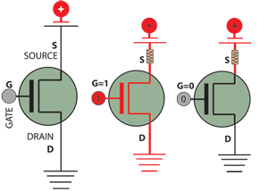
As we saw in the analysis of mathematical logics we’ve done so far, we are only interested to know if the electricity flows (1), or doesn’t flow (0). The transistors that can contemplate intermediate states don’t concern us. All or nothing, is what we are interested in.
We have also seen how the transistor allows us to obtain these two situations:
- With voltage applied to the Gate, or G=1, as shown in Figure 4 Center, the switch is closed and the electric current flows through the transistor.
- Without voltage applied to the Gate, or G=0, as shown in, the switch is opened and the electric current does not flow through the transistor.
As the transistor NPN was build so PNP transistor could have been, but we will use NPN in our work.
In order to replicate the physical behavior of a logical gate the transistors have to be connected into circuits. The first circuits were buid connecting the transistors with wires, some time after replaced by copper lines in printed boards (latter we’ll see what this is). The gates could be connected to each other. This was the integration of transistors into circuits.
As the complexity of the circuits grew and nanotechnology reduced the size of the transistors, the circuits with the transistors started to get build inside the same encapsulation, i.e. from integration of transistors into circuits we went to integrated circuits of transistors, or Chips.
So we reached Integrated Circuits, but we will only analyze them in the next article.