
Intel i7 Nehalem
We’ve chosen the Nehalem Intel architecture because it is the foundation of the Intel Core i7 CPU, a good example of what we can wait from a CPU in the present allowing us to predict what to wait in the closest future.
There’s lots to say about a so complex last generation CPU like this one. The changes it introduced in the motherboard organization, the solutions to the main bottlenecks who prevented the CPU performance, the new concepts about the connection with the memory, now incorporating a memory controller in the CPU chip and a lot more of questions that we will try to highlight and analyze along the chapters of this work.
For now we are going to focus our attention in questions related with the internal architecture of this CPU core and the way how it evolved to achieve the purpose of producing more μops per clock cycle, therefore in the parallelization of the instructions execution.
It will never be our purpose an exhaustive description of the functionality and architecture of this CPU. It would be too ambitious from us and for our present level of knowledge to detail such theme with the due correction.
What is important to withhold from the description we are going to do is what Nehalem architecture brought to the CPU evolution and what we can wait from them.
The Instructions Flow
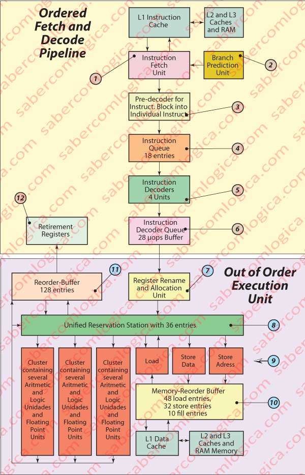
We’ll support this paragraph description in the graph of Figure 42
Intel Core i7 CPU uses the Intel64 instructions set, composed by macro instructions CISC (Complex Instruction Set Computer). The internal architecture of this CPU is composed by a set of RISC (Reduced Instruction Set Computer) micro operations (μops) .
Let’s summarize how is processed the instructions flow. The CPU:
- Fetches a set of de macro instructions, for instance a cache block.
- Pre-decodes these blocks into the different individual instructions that it contains.
- Decodes each of these instructions into μops and puts them into appropriate buffers in order to be dealt by a specific Functional Unit (FU).
- Dispatches the μops to an available FU (Functional Unit) as soon as they receive their operands.
- Retires the completed μops and saves their results permanently.
All this process is executed in a pipelined fashion by a 14 stage pipeline. To have the pipeline filled the Core i7 CPU allows the μops to be executed Out of Order. In order to achieve this purpose it uses:
- the Instructions Dinamic Scheduling, whose job is to decide which μops can proceed ensuring the correct program semantics
- the Instructions Speculative Fetch which loads the instructions from the program before the results of conditional branches are known. In order to achieve this goal, the Core i7 CPU uses a Branch Prediction Unit which tries to anticipate with the maximum precision the program conditional branches.
Once executed, the μops are retired and placed with their results in a Reordering Buffer or supply their results to other μops waiting for those results as the operands they need to be dispatched to a FU (Functional Unit). Once reordered, the μops are retired from the reorder-buffer and their results saved permanently, according with the program architecture.
All this complex Pipeline and Execution Engine have as their main goal to achieve the maximum rate of μops retired per Clock cycle.
Let’s now see with some detail all these components as well as the intermediate buffers which were created with the purpose of always having many μops available in all the dispatch points. To help us we will still use the same Figure 42. The notes (note x) that we will designate along the exposition always refer to this figure.
Ordered Instructions Fetch and Decode Pipeline
The Instructions Fetch Unit (note 1) fetches in cache L1 and always loads 16 Bytes blocks of aligned instructions. This unit executes the speculative instructions fetch, i.e. it loads speculatively instructions before it has the outcome of branch instructions and thus before the correct program path is determined.
The instructions executed out of order and in a speculative fashion may have to be canceled if an unpredicted branch shows that those instructions were in a wrong program path. In this situation all the speculative work done inside the pipeline is discarded with huge costs in terms of pipeline performance. This is why modern processors invest heavily in logic circuits in order to minimize wrong branch prediction.
For the speculative fetch to get instructions from the correct program path this unit gets support in the Branch Prediction Unit (note 2), whose task is to predict with the maximum precision the correct branches in the program execution before it has the outcome of a conditional branch instruction or even before direct or indirect calls and unconditional jumps.
The so obtained 16 Bytes block of aligned instructions is sent to a Pre-decoder (the Instruction Length Decoder) (note 3) whose job is to identify and sort out the individual instructions from the block and put them into the Instructions Queue Buffer (note 4), with 18 entries where the instructions wait in it’s original order to be dispatched to the Instruction Decoding Unit (note 5) containing 4 decoders with the ability to deliver to the μops Queue Buffer (note 6) up to 4 μops for each clock cycle.
Out of Order Execution
The μops are now prepared to be executed. But, if we wait for the necessary operands, since we are dealing with a 14 stages pipeline, we will certainly have lots of bubbles and frequently stall.
To surpass this question the Nehalem architecture executes the μops out of order. Speculatively, several μops of most advanced parts of the program, non dependent of μops from previous instructions in the natural sequence are executed and their results are kept in buffer waiting for the demands of the μops which will need them.
This way we can fill several stages of the pipeline with μops which will execute before those which are before them in the program natural order and prepare the data which will be necessary to the program execution in a most advanced part.
Let’s see with some detail the composition of the execution engine of the Core i7.
Our μops are waiting in the μops Queue Buffer (note 6), from where they will now be selected by the Register Rename and Allocation Unit (note 7) to the Execution Unit. This register executes tasks like:
- allocate resources to each μop (an entry in the Reservation Station, an entry in a load/store Buffer if a Memory Access is being made, an entry in the Reorder-Buffer),
- bind each μop to the appropriate dispatch channel,
- prepare the CPU internal architecture to work with the intermediate results, renaming the operands in an adapted way to internal registers non visible to the code and
- provide the operands which each μop needs, when available.
When this task is complete, the μops are delivered to the Unified Reservation Station (note 8), which can contain up to 36 μops waiting for their operands to be dispatched through 6 channels to 6 different Execution Units (EU) (note 9). This way up to 6 μops can be dispatched each clock cycle.
Three channels and their correspondent EU are designated to read and write data and addresses in memory. The other three channels are composed by Arithmetic and Logic Units (ALU) in different quantities.
One EU can contain several FU (Functional Units) (note 9), specifically several ALU for operations with com integers and/or Floating Point. The FU, specially those designated for more complex operations can be pipelined, what allows them, with the proper buffering of intermediate results, contain several μops simultaneously and even produce a result for each clock cycle.
The FU for memory access do it through the Memory Order-Buffer (note 10) which, supported in its separate retaining buffers ensures the consistency of writes and reads in memory.
The results of the μops processed by an EU can be sent back to the Unified Reservation Station as operands for waiting μops or delivered to the Reorder-Buffer (note 11) whose task, essential for the out of order execution success, consists in retaining the μops and retire them exclusively in the sequential order of the program macro instructions architecture. Once treated like this, it delivers the μops to the Retirement Registers (note 12), as these already work in the program architected order.
What’s new with Nehalem
This very little exhaustive but with some depth description had the sole aim to show how the Core i7 Nehalem architecture represents an evolution towards the instructions execution parallelization, in this case analyzed within each core.
The heavy investment in logic circuits is mainly:
- in the Branch Prediction Unit,
- in the deepest μops retaining buffers for the several phases of ordered fetch and out of order execution,
- in the creation of a great number of Functional Units in order to execute simultaneously several μops and
- in logic for the buffers which ensures the consistency of all the μops being executed out of order.
To all this we must add:
- a direct access to the Main Memory, through the incorporation of the Memory Controller into the CPU chip and
- a huge growth of the Cache Memory size, now with 3 levels, being the first 2 exclusive for each core and the third one for all the cores. We will deal with the Cache Memory latter on in its proper Chapter.
Anyone who wants a deeper knowledge about these and other features of Intel Core i7 can read the work used as base for our little synthesis, from Michael E. Thomadakis, Ph. D. from the Texas A&M University – “The architecture of the Nehalem processor and Nehalem-EP smp platforms” – in the link http://scholar.google.com/citations?view_op=view_citation&hl=en&user=p7WnungAAAAJ&citation_for_view=p7WnungAAAAJ:d1gkVwhDpl0C
Why More Transistors
We think the answer to this question is already given. Let’s see:
- Program branches prediction.
- μops Speculative and out of order execution.
- Data consistency insurance in out of order and parallel accesses to memory.
- ALU operations pipelined.
- Simultaneous execution of 6 μops in 6 EU with several different FU, some of them pipelined.
- Assurance that the final reorder of all this set of instructions executed in a disorganized manner, delivers a final result with instructions organized according to the program architecture.
- And a lot of other tasks which we won’t designate
Knowing this it’s easy for us to imagine the huge amount of logic which supports it. And when we say logic we refer to complex and high level programs embedded in the CPU chip. This logic is done with logical circuits, which are done with logical gates, which are done with transistors.
Here we are, finally. More transistors allow more logic.
In order to render the CPU more efficient and approach its maximum frequency, we must eliminate its bottlenecks.
The way Nehalem tries to do it is executing the μops in a pipelined fashion, with a 14 stage pipeline, and creating around it all the necessary and possible logic in order to avoid bubbles and stalls.
This path to the paralleled execution is still giving its first steps. But is definitely the path to follow. Nehalem didn’t solve everything, far away from that. Unblocking certain bottlenecks, other bottlenecks arose.
The search for the best solution proceeds, now trying to unblock the new bottlenecks, but all the steps to improve the profitability of the resources we already have will be done at the expense of many transistors, hundreds of millions of transistors. And we mustn’t forget that we are describing one of 4 or 6 cores of a CPU chip.
Conclusion
Much as the engineers are able to develop algorithms for parallelization, if the developers are not able to contribute with their technical and applied knowledge in the best way so that their programs fall within the proper premises, all the profitability will fail. Thus the importance for a developer to know how a CPU works and what’s important for it.
It’s also through the parallelization of parts of the programs, what we call threads, which is currently an heavy investment of CPU manufacturers, creating the multi-core CPU and all the necessary logic to ensure consistency for the operations developed in threads of the same program running in parallel on different cores. But this one depends mainly from the developers. For us to understand how the developers can use these technics in their programs, we have first to analyze the Operating Systems. They don’t manage the threads execution but they supply the tools for the developers to manage it.
The connection between the CPU and the Main Memory is absolute. Its using the Main Memory addresses that the CPU fetches all the instructions and data for a running program. This way, the CPU performance its dependent on the Memory system performance. That’s why we are going to analyze all the memory system behind a performant CPU.
But, the same way that the programs being executed are read from the HDD (Hard Disk Drive) to the Main Memory, the necessary parts of it for the CPU are read from the MM to the Cache Memory. The Cache Memory is the one where the CPU gets what it needs, but always using the Main Memory addresses. Confuse? Due the importance of knowing how such interconnection works, this is a theme that we will develop further on in appropriate Chapters about the Main Memory and the Cache Memory.
After that we will deal with the Operating Systems in another Chapter. These are the real commanders of the computers, those who establish the connection between our abstractions and the physical reality of the nowadays computer.
There we’ll add another concept of memory created and managed by the Operating System, the Virtual Memory, which will deal with the real memory for us. But let’s be cool. First we must see how the real one works and interconnects.
The CPU wouldn’t be very useful without all the peripherals which allow it to communicate with us, as for instance those who are called as human interface like the keyboard, the mouse, the joystick and the display, through which the CPU asks us for the data it needs to execute the programs and delivers us the result of their execution. But we must not forget all the other possible peripherals, among which we have the Main Memory and The HDD
How does the CPU communicate with all the possible peripherals and how does that communication work physically?
It’s a normal question at this point of our knowledge and important to be answered before we go further on.
The CPU only says what it wants and from whom. The management of all this communication is external to the CPU although always under its command. All the communication between the CPU and the world is done through the Motherboard, a printed board with several types of sockets where will connect all the peripherals and where a whole set of chips manages all the communication with the connected peripherals used by the CPU and using the CPU.
Therefore we believe that before we can discuss the Main Memory or the HDD (peripherals connected with the CPU through the motherboard) with more depth, we must make a brief description of what is a Motherboard and how it is composed.
The CPU simulation analyzed so far suited the only purpose to render easy to understand the logic of a CPU. We didn’t have in mind the clock frequency, which would be very low.
The Memory we considered was internal to the CPU chip and in direct connection with the CPU core circuits. Thus the values fetched by the CPU in memory were found as if they were in the internal CPU circuits.
From now on we’ll forget the CPU that is suited for our analysis and think of real CPU and real Memory and its system.
We’ll also do the analyzes to the basic computing unit, which is the byte. Any commercial CPU can address the byte or the word, whatever its size.
We would like to refer the book of Prof. Carlos Delgado from the Instituto Superior Técnico (Lisbon) – “Arquitetura de Computadores” as well as the articles that Engº Benito Piropo wrote in ForumPCs about “O Computador” – http://www.bpiropo.com.br/es_fpc1.htm from where we got the inspiration for the development of part of this Chapter.