
CMOS Transistors
CMOS Manufacture
The manufacture of these transistors is very similar to what we saw for the nMOS transistors. Let’s go through it step by step with the help of the tables in Figure 1-20.
The number of frames is much smaller because we decided to accumulate many manufacturing phases in each frame, essentially standing out the way of manufacturing one transistor comprising two opposite, nMOS and pMOS.
Frame 1 – The wafers taken from the silicon ingot are polished and cleaned of any impurities. 
Frame 2 – The wafer’s surface is oxidized. Silicon Dioxide (SiO2) is used as a protective layer to the ultra clean silicon wafer’s surface and also as an insulating layer.
 Frame 3 – (1)Deposition of Polysilicon layer followed by a Silicon Nitride (Si3N4) layer. (2)Deposition of a photosensitive and resistant to etching product layer over the above ones. (3)By a photolithography process the wafer is exposed to UV light through previously developed masks that define the location of the n-doped wells where the pMOS will be created. (4)Removal of the exposed photosensitive material.
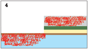
Frame 4 – (1)Removal by etching of Si3N4 and Polysilicon layers in the areas not protected by the photosensitive layer. In these areas SiO2 becomes exposed. (2)Bombardment and implantation of Phosphorus atoms, which penetrate through the thin layer of SiO2 being retained by Si3N4 in the areas where it was not removed. The Phosphorus atoms containing electrons in excess (more electrons than protons) provide the creation of a N (Negative) layer after its incorporation into the silicon crystal structure.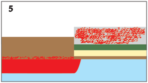
Frame 5 – (1)The ionization process is followed by an annealing process at high temperatures in order to reconstruct the crystal structures and incorporate the implanted atoms in it. Due to its diffusion the Phosphorus atoms are added to the wafer’s crystal structure, thus creating the n-doped well. (2)Deposition of another SiO2 much thicker layer over the SiO2 exposed layer. The protection granted by Si3N4 allows only the Polysilicon tops to be affected by this deposition, thereby protecting the parts of the wafer not to be affected.
Frame 6 – (1)Removal of the unexposed photosensitive material by a chemical own process. (2)Removal by etching of Si3N4 and Polysilicon layers below it. In these areas SiO2 becomes exposed. (3) Bombardment and implantation of Boron atoms, which penetrate through the thin layer of SiO2 being retained in the thicker layer of SiO2. The Boron atoms containing holes in its crystal structure (lack of electrons) provide the creation of a P (Positive) layer after its incorporation into the silicon crystal structure.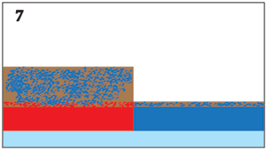
Frame 7 -The ionization process is followed by an annealing process at high temperatures in order to reconstruct the crystal structures and incorporate the implanted atoms in it. Due to its diffusion the Boron atoms are added to the wafer’s crystal structure, thus creating the p-doped well. 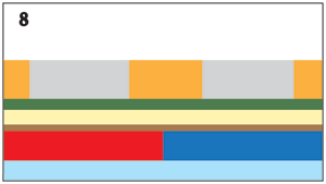
Frame 8 – (1)Total removal of SiO2 layers by etching. (2)Deposition of a renewed thin SiO2 layer. (3)Deposition of a Polysilicon layer followed by a Si3N4 layer. (4)Deposition of a photosensitive and etching resistant layer over the above ones. (5)Photolithographic exposition of the wafer to UV light through a mask that will reveal the zones out of the transistors.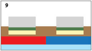
Frame 9 – (1)Removal of the photosensitive material exposed. (2)Removal by etching of the Si3N4 and Polysilicon layers in the areas not protected by the etching resistant material. In these areas SiO2 becomes exposed. (3)Deposition of an SiO2 much thicker layer over the SiO2 exposed layer.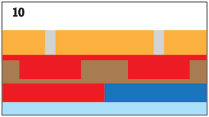
Frame 10 – (1)Removal of the unexposed photosensitive material by a chemical own process. (2)Removal by etching of Si3N4 and Polysilicon layers below it. In these areas SiO2 becomes exposed. (3)Removal of a thin part of the SiO2 layer and immediate deposition of a new SiO2 layer, in order that the SiO2 layer surface stays renewed and totally cleaned. (4)Deposition of an n-doped Polysilicon layer. (5)Deposition of a photosensitive and etching resistant layer. (6)Photolithographic exposition of this layer to UV light through a mask that defines the transistors’s gates.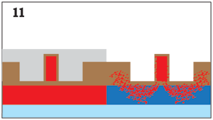
Frame 11 – (1)Removal of the exposed photosensitive material. (2)Removal by etching of the Polysilicon layer below it. This way the nMOS and pMOS transistors’s Gates are created in n-doped Polysilicon. (3)Removal of the unexposed photosensitive material by a chemical own process. (4)Removal of a thin part of the SiO2 layer and immediate deposition of a new SiO2 layer, in order that the SiO2 layer surface stays renewed and totally cleaned. The now defined transistors’s gates get insulated too. (5)Deposition of a photosensitive and etching resistant layer. (6)Photolithographic exposition of this layer to UV light through a mask that defines the nMos transistors’s sources and drains. (7)Removal of the exposed photosensitive material. (8)Bombardment with Arsenic atoms which penetrate in the wafer through the SiO2 thinner layer being retained by the SiO2 thicker layer. Arsenic atoms are preferable to Phosphorous atoms at this stage, as they allow a bigger concentration, thus a most equilibrated profile.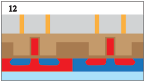
Frame 12 – (1)By an annealing process at high temperatures the crystal structures are reconstructed and the implanted atoms are incorporated in it. Due to its diffusion the Arsenic atoms are added to the wafer’s crystal structure, thus creating the nMOS transistors’s Sources and Drains. (2)Removal of the remaining photosensitive material. (3)Removal and reposition of a thin SiO2 layer, thus remaining renewed and clean. (4)Deposition of a photosensitive layer. (5)Exposition of this layer to UV light through a mask that defines the pMOS sources and drains. (6)Removal of the exposed material. (7)Bombardment wit Boron atoms. (8)Again by an annealing process the Boron atoms are added to the wafer’s structure. This way are now created the pMOS transistors’s Sources and Drains. (9)Removal of a thin SiO2 layer. (10)Deposition of a thick SiO2 layer which must cover all the elements executed until now. Its main function will be the insulation between the metallic connections that are going to be executed from now on. (11)Deposition of a photosensitive layer. (12)Exposition of this layer to UV light through a mask that defines the electrical circuit for the sources and drains of the transistors.
Frame 13 – (1)Removal of the exposed material. (2)Removal of the exposed SiO2 by etching, becoming exposed the wafer’s doped silicon. (3)Deposition of a metal layer which will fill the opened holes and establish the connections between the Sources and Drains of the different transistors. (4)Deposition of a photosensitive layer. (5)Exposition of this layer to UV light through a mask that defines the electrical circuit at this layer’s level .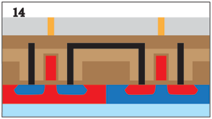
Frame 14 – (1)Removal of the exposed material. (2)Removal by etching of the metallic material now exposed. (3)Removal of the remaining photosensitive material. This way remains defined an electrical circuit connecting the sources and drains of the nMos and pMOS transistors, interconnecting them as CMOS transistors and connecting the CMOS with each other. (4)Deposition of a thick layer which will cover all the metallic circuit, acting as its insulator. (5)Deposition of a photosensitive material layer. (6)Exposition of this layer to UV light through a mask that defines the places where the transistors’s gates are.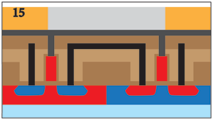
Frame 15 – (1)Removal of the exposed material. (2)Removal of the exposed SiO2 by etching, becoming exposed the gates’s n-doped silicon. (3)Removal of the remaining photosensitive material. (4)Deposition of a metal layer which will fill the opened holes and establish the connections with the Gates. (5)Deposition of a photosensitive layer. (6)Exposition of this layer to UV light through a mask that defines the electrical circuit at the Gates level.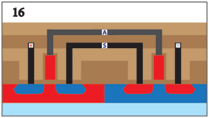
Frame 16 – (1)Removal of the exposed material. (2)Removal by etching of the metallic material now exposed. (3)Removal of the remaining photosensitive material. This way remains defined the electrical circuit of the transistors’s Gates. This circuit is represented in Grey color, meaning that it is at a different plan from the first one. Deposition of a last SiO2 insulating layer for this metallic, for the transistors and the chip where they are integrated.
CMOS Logic

The CMOS transistors are composed by two nMOS and pMOS combined transistors.
In Figure 1 we can see the graphic representation for the nMOS and for the pMOS transistors.
Being VDD the power supply voltage:
- nMOS transistor is conductive when its Gate is supplied with voltage between VDD/2 and VDD or the equivalent logical value 1.
- pMOS transistor is conductive when its gate is supplied with a voltage between 0 and VDD/2 or the equivalent logical value 0.
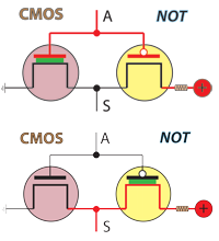
The CMOS transistor alone is an inverter, i.e. a NOT logical gate. We’ll just understand why analyzing its logic in Figure 2, where we can see its graphical representation.
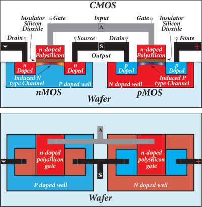
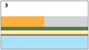
In Figure 3 we intend to illustrate the transition between the CMOS graphic representation and its graphic representation as it will be in silicon. We show its representation in section and in plan, so that we can understand how the metallic connections work in different sections.
In a CMOS transistor, the pMOS source is connected to the supply and the nMOS drain is connected to ground. The pMOS drain and the nMOS source are connected each other and CMOS output S is embedded in this connection. The input A is connected to both of the nMOS and pMOS gates.
- When A is 1, nMOS is conductive and pMOS is insulator. As pMOS source is connected to power the electrical stream doesn’t flow through CMOS transistor, thus its output S is 0.
- When A is 0, pMOS is conductive and nMOS is insulator. As pMOS source is connected to power the electrical stream flows through it and its connection with nMOS, which is insulating. Thus the electrical stream flows through the CMOS output S, so being 1.
CMOS NAND Logical Gate
As we have seen, the physical behavior of a NAND logic gate was achieved by the serial connection of two nMOS transistors, for the chosen circuit.
In the case of CMOS transistors, since the issue is not so simple, as we said such a basic visual approach it’s not possible to explain the NAND materialization. Let’s see.
With a NAND logical gate we want the output 1 when one or both inputs are 0.
When a CMOS transistor has one of its components as a conductor the other will be an insulator.
It’s through the pMOS transistors that CMOS is connected to the power supply.
As the pMOS is conductive with 0 at its gate, for the CMOS to be powered on with at least one of the inputs with the value 0, two pMOS connected in a parallel fashion to the power supply will do the task.
For this to be reflected in the output, it is necessary that in any of the referred situations the electrical current doesn’t flow to ground.
In the situations described, when both inputs are different one of nMOS is conductive. So we must ensure that both nMOS must be conductive (both inputs at 1) in order that the electric stream can flow to ground. If we connect them in a serial fashion to ground, that will do it.
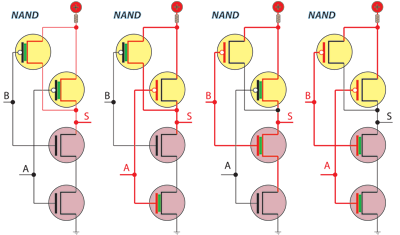
We have found the solution. Now we need to connect the two CMOS to each other so that they meet the described, as we can see in Figure 4.
Thus we can conclude that:
To get a NAND gate with CMOS transistors we must use two CMOS connected each other so that:
- the two nMOS are connected in serial to the ground
- the two pMOS are connected in parallel to the power supply, i.e. both connected to the power supply.
CMOS NOR Logical Gate
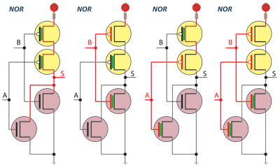
As we have seen, the physical behavior of a NOR logic gate was achieved by the parallel connection of two nMOS transistors, for the chosen circuit.
In the case of CMOS transistors, since the issue is not so simple, as we said such a basic visual approach it’s not possible to explain the NOR materialization. Let’s see.
We want the output to be 0, always one or both inputs have the logical value 1.
It’s through the pMOS that the CMOS transistors are connected to the power supply.
As the pMOS is conductive with 0 at its gate, the CMOS will always be powered on when at least one of the inputs is 1. And this is just what we don’t want to happen.
Well, it’s easy. If both pMOS are connected in a serial fashion to power supply that doesn’t happen, for both they need to have their gates at 0 to be conductive, thus powering on the CMOS.
And this is just what we want.
Whenever the output is 0, the nMOS transistors must ensure grounding, so that this state can not be influenced by any noise.
But as we have seen, when the output is 0 one of the nMOS gates can have the value 0, being an insulator.
To prevent this, if we connect both nMOS to ground in a parallel fashion, we ensure that it will be enough one of them to be conductor in order to grant any tensions runoff.
In the case where the two inputs are 0, both pMOS are conductors and both nMOS are insulators, so that the output is 1.
We have found the solution. Now we need to connect the two CMOS to each other so that they meet the described, what is reflected in Figure 5.
Thus we can conclude that:
To get a NOR gate built with CMOS transistors we must use two CMOS connected each other so that:
- the two nMOS are connected in parallel to the ground
- the two pMOS are connected in serial to the power supply.
Conclusion
We consider here for concluded this Chapter about the materialization of logical gates. Until this point of evolution we have already noticed that the concepts of Boolean algebra and logical gates can solve everything on a computer. We have even materialized in electrical circuits the behavior of these logical gates.
We realized what to do with all this vermin, the question we left at the end of the Chapter in which we spoke about bits. Actually, all this vermin is walking through the computer circuits turning on and off switches.
Symbolically, the bits, the smallest unit of information, through its state of 1 or 0 meaning with or without voltage, are sent by the computer circuitry connecting or disconnecting transistors (taking or not voltage to their Gates) returning with the response of the circuit they crossed, or doing the same job into external circuits (OUT) or from external circuits (IN).
And how does that make arithmetic operations, puts images on screen and sounds in the loudspeakers?
Be cool. One thing at a time. Let’s first highlight what we found so far. All logical gates electric representations were made from NOT, NAND and NOR circuits, as indeed we made sure to highlight. And all circuits that we will analyze from now on will be built by combinations of the logic gates which we addressed so far, therefore combinations of NOT, NAND and NOR.
As we said, the great complexity comes from the most elementary simplicity, if we descend to the base and evolve by combinations of what we have analyzed. Complex is the development of logical reasoning which allow us to create the combinations that solve the problems we want. The key is to understand the functionality of each circuit, the only way we can use them included in logical combinations, i.e. in more complex algorithms. In mathematical logic and computing the limit is our imagination.
Let’s now understand how the computer does arithmetic.