Integrated Circuits (Chips)
In order to replicate the physical behavior of a logical gate the transistors have to be connected into circuits. The first circuits were buid connecting the transistors with wires, some time after replaced by copper lines in printed boards (latter we’ll see what this is). The gates could be connected to each other. This was the integration of transistors into circuits.
As the complexity of the circuits grew and nanotechnology reduced the size of the transistors, the circuits with the transistors started to get build inside the same encapsulation, i.e. from integration of transistors into circuits we went to integrated circuits of transistors, or Chips.
The processors are the most well known form of Chips, where nowadays about 2 billion transistors are incorporated in a Chip with about 1 cm2.
Let’s look the nMOS transistors as switches and build the electrical circuits which will execute physically the logical gates behavior, which are the physical visualization of the Boolean operators abstraction.
But first we are going to see the manufacturing process of transistors inside a CHIP.
How an IC with nMOS is made
We will now realize the process of manufacture of nMOS transistors circuits. The development of an Integrated Circuit (IC) begins with the study of the circuit by the engineers according to the desired solution.
Once finished its design and layout, it is decomposed in different masks that will be needed at the several stages of implementation.
The Wafer is the main element used in the manufacture of the chips. It’s on the wafer that the transistors giving rise to the Integrated Circuit will be implanted. The “virgin” wafer is made of pure silicon, which can be extracted from the sandy beach and liquefied at high temperatures.
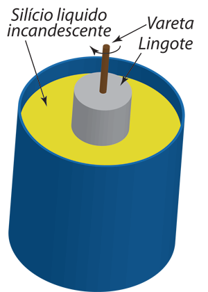


A piece of silicon crystal is placed on a stick and then dipped into molten silicon. The stick is suspended and rotated while forming a large silicon crystal cylinder, also known as Ingot.
The ingot measures one to two meters in length and can be up to 300 mm diameter. The ingot is “sliced” into wafers which go to production.
In each wafer are manufactured hundreds of IC (chips) i7 microprocessor type, for example, with more than 700 million transistors each in its Nehalem architecture. This was possible thanks to the ability of producing 45 nm transistors, presently 22 nanometers.
Just to give you an idea of the physical nanometer, when in the beach, just pick up a grain of sand and imagine all the Portuguese coast, about 1,000 Km. This is the relationship between 1 nanometer and 1 meter.
Frame 1 – The wafers taken from the ingot of silicon are polished and cleaned of any impurities. This is one of the critical parts of the process.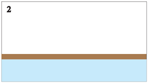
Frame 2 – This step consists in the oxidation of the surface of the wafer. Silicon dioxide (SiO2) is a very stable material. It is used as protection layer to the surface of the ultra clean silicon wafer and as an insulating layer. The SiO2 is formed at high temperatures in a furnace with oxygen atmosphere (dry oxidation) or in steam environment (wet oxidation). This process is called silicon’s oxidation. It’s like creating a layer of rust on iron, only much faster. The SiO2 is the main component of glass, which is obtained by heating it at high temperatures. 
Frame 3 – This step consists in the bombardment and implantation of boron atoms in the silicon over the entire wafer in an extremely uniform manner, controlled, and with low intensity, so that the formed P layer were regular and not very intense. Boron Atoms cause gaps in the structure of silicon atoms (less electrons than protons) creating the P layer (positive).
Frame 4 – Again a new boron atom bombardment, even less intense in order to put the voltage in the surface layers in the desired threshold.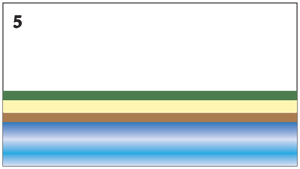
Frame 5 – Because one of the main requirements of this process is the extremely high quality and cleanliness of the surfaces to work, the layer of silicon dioxide is removed by a process called etching.
Etching consists in attacking a particular element (provoke its corrosion) by particles in a liquid or gaseous component. It can be done by Wet Etching, which is chemical, or by Dry Etching, which is done in plasma reactors.
After its remotion a new thin layer of SiO2, totally renewed, is created, followed by the deposition of a polysilicon layer and the deposition of a silicon nitride (Si3N4) layer. This deposition is performed in a high temperature furnace through the deposition of gas steam.
Both the semiconductor layers, the insulating and the conductive, can be formed inducing the deposition of selected gases at high temperatures. The chemical steam deposition can produce solid films of high quality.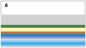
Frame 6 – In the next step, a layer of a photosensitive and etching resistant product is deposited.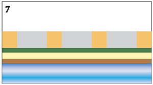
Frame 7 – By a photolithography process the wafer is exposed to UV light through one of the masks previously developed by the engineers who designed the IC. The exposure of the photosensitive material to ultraviolet light changes its characteristics, allowing its removal in the exposed areas, what is done.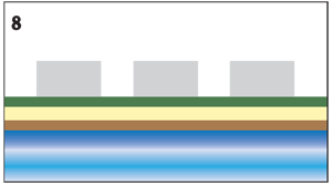
Frame 8 – Once again by etching, the layers of Si3N4 and polysilicon are removed in the areas not protected by the photosensitive layer. In these areas SiO2 layer stays exposed.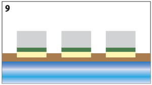
Frame 9 – The wafer is exposed to an oxidizing atmosphere and the subsequent creation of a much thicker layer of silicon dioxide in he areas where the first SiO2 layer was exposed. The remaining wafer areas are protected by the photosensitive material, being only affected the tops of polysilicon not protected by Si3N4.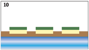
Frame 10 – The remaining unexposed photosensitive material is removed by a unique method of the material itself.
Frame 11 – Again by etching, Si3N4 and polysilicon layers, now unprotected, are removed.
Yet by etching is superficially removed a piece of SiO2 layer which is immediately reset by oxidation, thus leaving a quite clean and refreshed surface.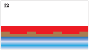
Frame 12 – Immediately after oxidation, a polysilicon N doped layer is created, by atom bombardment or diffusion of phosphorus through the gas that originates the layer.
The addition of phosphorus atoms generates free electrons in the silicon structure affected.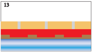
Frame 13 – After the deposition of another layer of photosensitive material a new photolithography process is executed, using other masks which define the gates of the transistors.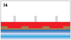
Frame 14 – The exposed photosensitive material is removed, leaving exposed the underneath polysilicon areas.
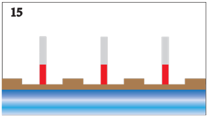 Frame 15 – By etching, the exposed polysilicon is removed. This way, it remains the transistors’s gates executed in N doped polysilicon.
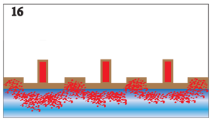
Frame 16 – This frame illustrates several stages.
Removal of the remaining photosensitive material.
Surface cleaning by etching of the exposed SiO2, immediately reset by oxidation, thus leaving a quite clean and refreshed surface, now also protecting the gates.
Bombardment with phosphorus or arsenic atoms. Arsenic is preferable at this stage for it allows a greater surface concentration and a more balanced profile. The atoms penetrate through the thin layer of silicon dioxide but are retained by the thicker layer.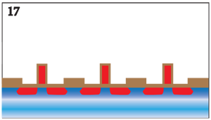
Frame 17 – Each ionization must be followed by an annealing process at high temperatures in order to reconstruct the crystal structures and incorporate the atoms implanted in the crystal structure. Due to its diffusion, the arsenic atoms are added to the wafer’s structure.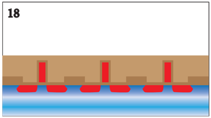
Frame 18 -Contacts are needed to interconnect the individual devices and form an IC. For a better insulation between the transistors and future connections of metal, a thick layer of SiO2 covering all the wafers is deposited.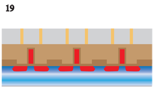
Frame 19 – This frame includes the deposition of a photosensitive material layer of over and another process of photolithography that exposes it to UV light through a mask that defines the electrical connection points of the sources and drains of the transistors.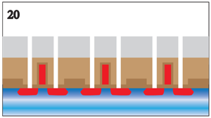
Frame 20 – The exposed photosensitive material is removed. Through etching SiO2 is removed until the N doped silicon wells which define the sources and the drains of the transistors.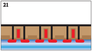
Frame 21 – A layer of metal, e.g. aluminum, that will fill the open holes and establish the contacts with the transistors’s sources and drains, is deposited.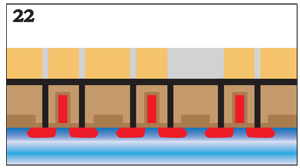
Frame 22 – Once again a layer of photosensitive material is deposited and then exposed to UV light through a mask that defines an electrical circuit at this level.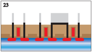
Frame 23 – The exposed photosensitive material is removed. Then, and again by etching, the exposed metal is removed. Right away, the photosensitive material leftover is removed by its own method.
After these operations is defined a circuit which uses some or all of the transistors sources and drains manufactured before. The part of the circuit that we can see is the one in our cutting plan, but the connections are transverse and longitudinal along the whole wafer.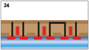
Frame 24 – In complex circuits several metal layers in different levels will exist. In our case we will make one more circuit intended for the gates of the transistors. Thus, a thick layer of silicon dioxide, whose purpose is to isolate all contacts so far, is deposited.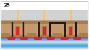
Frame 25 – Once again, a photosensitive material layer is deposited, and afterwards submitted to a photolithography process with a mask that defines the points of contact with the gates.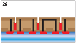
Frame 26 – The exposed photosensitive material is now removed and silicon dioxide which in consequence becomes exposed once again is removed by etching leaving the N doped polysilicon of the gates exposed. Finally, the remainder of the photosensitive material is removed.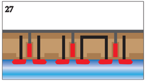
Frame 27 – Another metal layer (e.g. aluminum) which will fill all the contact holes opened is deposited.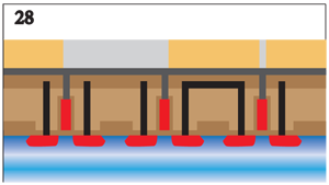
Frame 28 – A photosensitive material layer is deposited over the metal layer. Again by a process of photolithography and through another mask with the circuit of the transistors’s gates the photosensitive material is exposed to UV light.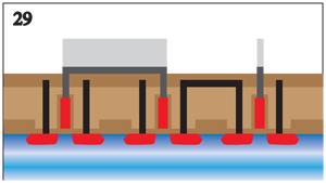
Frame 29 – The exposed photosensitive material is cleaned. By etching, the exposed metal areas are removed. The remaining portion of the photosensitive material is removed.
After these operations is defined a circuit which uses some or all of the transistors’s gates manufactured before.
The connections of this circuit are symbolize in grey because they exist in a different plan of our cutting one.
The part of the circuit that we can see is the one in that other plan, but the connections are transverse and longitudinal along the whole wafer.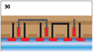
Frame 30 – Finally, a thick layer of silicon dioxide which is intended to insulate and protect the chip, is deposited.
And the wafer is ready. The next procedures are the cut and separation of all the chips included in the wafer, the connection of their terminals to the pins and their encapsulation.
After undergoing testing and verification processes, the Chip is ready to go into the commercial market.
