The Main Memory
The Main Memory or RAM as it is commonly known, has a name well longer than that, currently DDR3 SDRAM, i.e. Synchronized Dynamic Random Access Memory with Double Data Rate of 3rd generation.
Synchronized (S) because the memory clock is synchronized with the Motherboard via the Memory Controller ( MC) .
Dynamic (D) because the main memory is composed by cells that have a dynamic behavior , i.e. they have to be permanently charged. The SDRAM memory cell comprises a transistor and a capacitor. It’s the capacitor that stores the bit value (1 is loaded and 0 is unloaded) . But the capacitors lose their charge, thus having to be periodically recharged. Hence the name of Dynamic given to this memory.
RAM stands for Random Access Memory, i.e. we can access any cell in any address without having to scroll through the previous or the following or even any predefined sequence.
DDR3 stands for Double Data Rate or Double Transfer Rate level 3 .
As we’ll see, managing an SDRAM is complex, due to the large number of different operations that have to be carried out on it to ensure that its main operation, to store data for the CPU operation, can be efficiently accomplished.
To deal with this complexity there is the Memory Controller (MC), responsible for sending signals to the memory that will tell it the different types of operations to perform, how and when.
We will not analyze the MC as this is outside the scope of this chapter, but we will analyze how the memory performs and interprets the command signals sent by the MC .
We’ll see how the memory is physically organized and how we can individually access each one of the billions of cells.
We’ll see the shape and operation of a memory cell, the one that contains the bit value. How does a nano capacitor for its charge to be read or kept, when we know that its capacitance is less than the one of the lines he must feed in order to be read and restored. And how does it for that same charge to feed the circuit boards lines, these being not nano lines, instead micro copper lines, so that the information it contains arrives at its intended destination.
In other words, how does a small bucket dumped into a brook and then into a river, for its charge to be pointed out in that river, i.e. how can someone looking to the river know if the bucket was full or empty? And how do we for the bucket, after having being dumped into the brook for the river to know what it contained, to be kept as it was before being dumped, i.e. able to tell again what its charge is, because the value stored in the memory cell can not be lost just because it is read.
Let’s see how logic circuits such as Sense Amplifier and Buffer Tristate can fulfill the necessary functions in order to turn possible what we described in the previous paragraph.
What is a memory latency, i.e. the time we have to wait between the request of a given value and the response to be in the DIMM pins.
From where comes that latency value and why did it change so little since the first SDRAM to the recent models compared to the great transfer rates increase .
We will try to reproduce an imaginary SDRAM control circuit that meets the various operations to be performed by it and we’ll try to understand what they are, what purpose they serve and whether circumstances in which they are performed, trying to detail each of them in parts of the main circuit in which each function is fulfilled.
In memory, the clocked logic plays a fundamental role, so it will be treated with maximum possible depth , presenting charts with the clock several states (low, rising edge, high and falling edge), trying to link them with the different control signals, when they arrive and when they are processed in memory.
Therein we’ll highlight the different latency components which shall be respected as memory parameters, each one with their own, which are communicated to the MC as soon as it is turned on.
We will also try to understand what are the main differences between the successive SDRAM developments , DDR , DDR2 and DDR3 , who mistakenly are pointed as having very high frequencies when actually the internal memory working frequency is slightly different from the described SDRAM (depending on the model), being the BUS frequency the one which grows as it is injected with data up to 8 times per internal memory clock cycle, thereby achieving much larger transfer rates for the memory DIMM (not frequencies).
See the global synopsis of this work
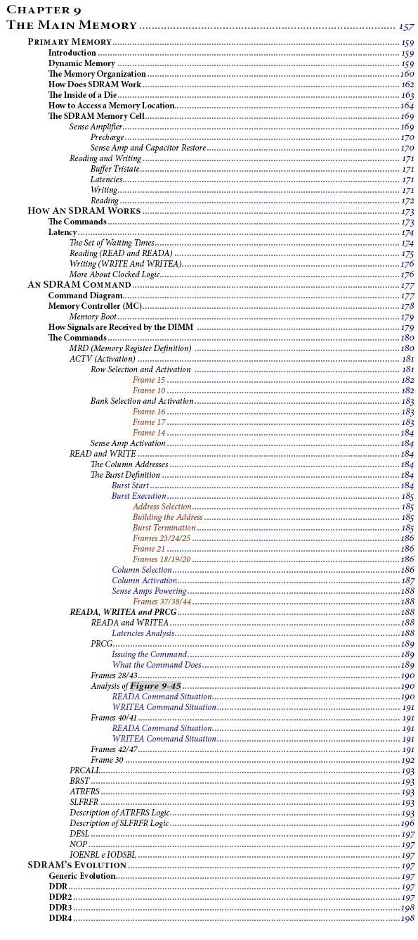
We introduce here the table of contents of the Paper Book to describe the themes approached in this Chapter

